Monday, November 12th 2018

AMD "Zen 2" IPC 29 Percent Higher than "Zen"

AMD reportedly put out its IPC (instructions per clock) performance guidance for its upcoming "Zen 2" micro-architecture in a version of its Next Horizon investor meeting, and the numbers are staggering. The next-generation CPU architecture provides a massive 29 percent IPC uplift over the original "Zen" architecture. While not developed for the enterprise segment, the stopgap "Zen+" architecture brought about 3-5 percent IPC uplifts over "Zen" on the backs of faster on-die caches and improved Precision Boost algorithms. "Zen 2" is being developed for the 7 nm silicon fabrication process, and on the "Rome" MCM, is part of the 8-core chiplets that aren't subdivided into CCX (8 cores per CCX).

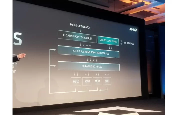
According to Expreview, AMD conducted DKERN + RSA test for integer and floating point units, to arrive at a performance index of 4.53, compared to 3.5 of first-generation Zen, which is a 29.4 percent IPC uplift (loosely interchangeable with single-core performance). "Zen 2" goes a step beyond "Zen+," with its designers turning their attention to critical components that contribute significantly toward IPC - the core's front-end, and the number-crunching machinery, FPU. The front-end of "Zen" and "Zen+" cores are believed to be refinements of previous-generation architectures such as "Excavator." Zen 2 gets a brand-new front-end that's better optimized to distribute and collect workloads between the various on-die components of the core. The number-crunching machinery gets bolstered by 256-bit FPUs, and generally wider execution pipelines and windows. These come together yielding the IPC uplift. "Zen 2" will get its first commercial outing with AMD's 2nd generation EPYC "Rome" 64-core enterprise processors.

Update Nov 14: AMD has issued the following statement regarding these claims.
As we demonstrated at our Next Horizon event last week, our next-generation AMD EPYC server processor based on the new 'Zen 2' core delivers significant performance improvements as a result of both architectural advances and 7nm process technology. Some news media interpreted a 'Zen 2' comment in the press release footnotes to be a specific IPC uplift claim. The data in the footnote represented the performance improvement in a microbenchmark for a specific financial services workload which benefits from both integer and floating point performance improvements and is not intended to quantify the IPC increase a user should expect to see across a wide range of applications. We will provide additional details on 'Zen 2' IPC improvements, and more importantly how the combination of our next-generation architecture and advanced 7nm process technology deliver more performance per socket, when the products launch.
Source: Expreview
Add your own comment

162 Comments on AMD "Zen 2" IPC 29 Percent Higher than "Zen"

#76
GoldenX
Buying AM4 was the best choice.
Posted on Reply
#77
bug
GlacierNineWe disagree in that you think it is reasonable for Intel to consider a 9900K as "working according to spec" at 3.6GHz and "Overclocked" at 4.7GHz, when clearly these products are actually designed to run at higher clocks, and are expected to by consumers, and *will run* at higher clocks, it's just that it is only achievable at a *much* higher TDP than intel claims their CPU actually has.
Clearly? Are you sure about that?
GlacierNineThey can't have their cake and eat it - Either the 9900K is "The world's fastest gaming CPU (At 150W TDP)", or it is a 95W part (but isn't anywhere close to being the fastest gaming CPU at that TDP).
There's no either/or here. It's both/and.
It used to be easy to say this CPU is better than that CPU when CPUs had a single core. It's become more complicated ever since.
Posted on Reply
#78
Turmania
I want at least 5ghz on all cores from new 2700x equivalent.15-20% ipc gain. Then I'm sold.Am I asking for too much? I do no think so considering Intel has not played die shrink hand yet but will do late in 2019.they probably will reach 5.5ghz plus.I want all AMD with cpu and gpu and use a free sync monitor.but AMD has to show me something for me to depart with my money.
Posted on Reply
#79
GlacierNine
bugClearly? Are you sure about that?


There's no either/or here. It's both/and.
It used to be easy to say this CPU is better than that CPU when CPUs had a single core. It's become more complicated ever since.
1 - Yes, yes I am sure about that.

2 - Intel wants to claim it can be the fastest gaming CPU while being 95W TDP. That's simply not true. It's 95W, or it's fast. One or the other.

It's not a 95W part at the same time as being the fastest gaming CPU.
It's not the fastest gaming CPU at 95W.

Why are you so insistent on defending their clear attempt to advertise a dichotomous product in a misleading way? What do you get out of refusing to admit that Intel's CPU draws as much power as it actually does?
Posted on Reply
#82
WikiFM
Vayra86Should have... would they be able to? A new node enables a new design I think and the compromises to do it on 14nm would kill the advantage anyway. 14nm is clearly pushed to the limit, and even over it for some parts if you look at their stock temps, (9th gen hi).

Eh... IPS in my mind is In Plane Switching for displays.
He spelled it fine, you didn't read it right
AMD increased IPC with each iteration of Bulldozer, all of them 32/28 nm. So why couldn't Intel increase IPC in 14 nm?
About the temps, by increasing IPC Intel could reduce clocks and still have higher performance with lower temps.
Smartcom5Gosh, I'm really sorry, was my bad!
Picked the wrong quote, was meant to quote @WikiFM

Smartcom
I said single threaded or IPC not because I think they are the same, but because Intel beats AMD in both.
Posted on Reply
#83
R0H1T
WikiFMAMD increased IPC with each iteration of Bulldozer, all of them 28 nm. So why couldn't Intel increase IPC in 14 nm?
About the temps, by increasing IPC Intel could reduce clocks and still have higher performance with lower temps.


I said single threaded or IPC not because I think they are the same, but because Intel beats AMD in both.
You mean once on 32nm & twice on 28nm? As for Intel ~ remember Tick Tock, which is now Tick Tock Tick Tick Tick :laugh:

Lisa Su said that work on Zen2 began 4 years back, sometime after that they would've realized that their vision could only be fulfilled on 7nm. Like wise for Intel they've been working on Icelake for 4~6 years & even if one assumes it could theoretically be backported to 14nm+++ that simply wouldn't work without major compromises to the final design. Just an FYI retail chips are rumored to feature AVX512, which is simply not possible on this node. That IPC gain includes a hefty one time benefit from AVX512.
Posted on Reply
#84
sideside
randomUserThis means, that:
Zen1 will handle 1 instruction per 1 clock ...
Yeah but as usual whoever wrote this has no idea what IPC is, virtually everyone uses it incorrectly.
Posted on Reply
#85
Vayra86
WikiFMAMD increased IPC with each iteration of Bulldozer, all of them 28 nm. So why couldn't Intel increase IPC in 14 nm?
About the temps, by increasing IPC Intel could reduce clocks and still have higher performance with lower temps.


I said single threaded or IPC not because I think they are the same, but because Intel beats AMD in both.
Because architecture isn't bound to a node but to a design. A viable architecture can scale as the nodes get smaller - Core and Zen represent such architectures.

The real story is told by IPC advances within the Core architecture and those are so massive, they are responsible for the lead AMD is still working to catch up on. Intel's main issue with Core is that they pulled out all the stops already with Sandy Bridge, and it was so strong, it remains relevant to this day. This is also why I among others say that Core has reached its peak and it needs radical changes to remain relevant. Its the same with GCN. Everything shows that it has been stretched to the max.

The story with Bulldozer is different and its remarkably similar to how they approach GPU up to today: as an iterative work in progress. You basically buy something that isn't fully optimized, and then you get to say 'ooh aah' every time AMD releases an update because performance increased. Unfortunately when the competition does go all the way, that means you end up with inferior product where optimization always trails reality.
Posted on Reply
#86
Smartcom5
ValantarHow I envision AMD's Zen2 roadmap:
[…]
Of course, this is all pulled straight out of my rear end. Still, one is allowed to dream, no?
Can I beat that please? Since I dreamed about Intel being at least somewhat competent all out of a sudden too!
Intel could – and I want that being understood as my forecast for their oh so awesome and totally revealing event on December 11th (hint: It won't be …) – they could help themselves quite a bit, if they just blatantly copy AMD's Fineglue. Whereas I strongly guess, that they will do exactly this;

How I'm envision Intel's near future roud-map:

Prediction:
For the consumer-market, Intel copies AMD's (UMI's?) HBM-alike MCP-approach and starts to manufature CPUs being glued-together (hurr, hurr) from complete and rather unchanged unaltered common CPU-Dies using QPI UPI, like two dual-core and quad-core Dies on a single chip – pretty much what they're about to do now with Cascade Lake in the server-space. So a rather common approach on unaltered MCP-level, just whole Dies combined unaltered at PCB-level.

After that, Intel in their second coming copies AMD on technology-level (once again) in the direction of a 'clustered CPU' and starts with a modular assembly using chiplets of different manufatured node-sizes too, connected (optimally hopefully) via their EMIB. That way they would be able to manufacture tiny core-chiplets which shall be reduced to e.g. only 4 cores per chiplet (or just 2 cores or even a single one). Such embodied pure-core chiplet or core-complex would be so tiny, that Intel could fab such chiplets hopefully even on their broken totally working on track™ 10nm node.

That way, they wouldn't have to give up their ardently loved black hole called iGPU too (or how I like to call it: »Adventures of The Mighty Blue Electron facing Competition: The Road towards Iris-Graphics«), while still bringing it in as a dedicated modular chiplet on e.g. 22nm 14nm.

So, tiny dedicated and independent core-complexes for the CPU-core part – let's call them CCi for now (Core Complex Independency) – while bringing in the rest of it on 14nm or even 22nm (given that their 28 nm process stopgap isn't still running yet …). All that as a modular Cluster-CPU put glued-together on actual Die-level as chiplets.

But seriously, ... that way, a) Intel could save their own ass over the time-span while they literally has nothing left (to lose) until they come up with their a hopefully newly revamped architecture, b) use and thus save their disastrous 10nm-fiasco (without the obvious need to just write it off [since for anything more than a Dual-core that node's yields are evidently out for the count]) and they c) even would come down from their insanely expensive monolithic Die-approach while even saving huge manufacturing- and processing-costs and thus d) increase profits.

Sounds quite like a plan, doesn't it?! Actually like a real epic masterplan I must say! I wonder why no-one else hasn't come up with such brilliancy yet?! … oh, wait!

Well, one can dream, can I?
Anyway, I'm thrilled!


Smartcom
Posted on Reply
#87
WikiFM
R0H1TYou mean once on 32nm & twice on 28nm? As for Intel ~ remember Tick Tock, which is now Tick Tock Tick Tick Tick :laugh:

Lisa Su said that work on Zen2 began 4 years back, sometime after that they would've realized that their vision could only be fulfilled on 7nm. Like wise for Intel they've been working on Icelake for 4~6 years & even if one assumes it could theoretically be backported to 14nm+++ that simply wouldn't work without major compromises to the final design. Just an FYI retail chips are rumored to feature AVX512, which is simply not possible on this node. That IPC gain includes a hefty one time benefit from AVX512.
You are right 32 nm too(Vishera and Piledriver), plus 28 nm(Steamroller and Excavator), 4 iterations.
Skylake-X has AVX512 in 14 nm, so mainstream AVX512 in 14 nm can be possible.
Posted on Reply
#88
bug
qcmadnesswww.anandtech.com/show/13544/why-intel-processors-draw-more-power-than-expected-tdp-turbo
I have read that very article. It says the CPU is built to run at 95W by default, but that TDP can be adjusted to squeeze more juice out of it.
Maybe people have been unaware till now, but this a trick that has been employed for a while by both Intel and AMD. The only thing that changed is Intel decided to put fewer numbers on the box. The numbers were apparently easily accessible to the people that wrote that article, so it's not like Intel keeps them secret.
GlacierNine1 - Yes, yes I am sure about that.
My apology, I didn't know you had the power to decide what's reasonable and what's not reasonable around here.
GlacierNine2 - Intel wants to claim it can be the fastest gaming CPU while being 95W TDP. That's simply not true. It's 95W, or it's fast. One or the other.

It's not a 95W part at the same time as being the fastest gaming CPU.
It's not the fastest gaming CPU at 95W.

Why are you so insistent on defending their clear attempt to advertise a dichotomous product in a misleading way? What do you get out of refusing to admit that Intel's CPU draws as much power as it actually does?
I didn't realize you know what Intel wants to claim either.

To me this is extremely simple: people are stupid, you put more than one number on the box, they get confused. Intel realized that and decided not to put several TDPs on the box anymore.
For those genuinely curious about the platform and how to properly tweak it, all the info is right here: www.intel.com/content/www/us/en/products/docs/processors/core/8th-gen-core-family-datasheet-vol-1.html (search for PL2)
Posted on Reply
#89
Smartcom5
Isn't Cannon Lake's infamous i3 8121U their first CPU within the mainstream space which features AVX-512 already?

Edit: @bug That TDP-classification of just 95W still is just deceptive …
Though that was without question the whole intention from the get-go when they started rating it that way, based on base-clocks.
It was an (working) approach to make look their chips more energy-efficiency while the efficiency of those chips didn't really changed at all.


Smartcom
Posted on Reply
#90
Daven
bugI have read that very article. It says the CPU is built to run at 95W by default, but that TDP can be adjusted to squeeze more juice out of it.
Maybe people have been unaware till now, but this a trick that has been employed for a while by both Intel and AMD. The only thing that changed is Intel decided to put fewer numbers on the box. The numbers were apparently easily accessible to the people that wrote that article, so it's not like Intel keeps them secret.


My apology, I didn't know you had the power to decide what's reasonable and what's not reasonable around here.


I didn't realize you know what Intel wants to claim either.

To me this is extremely simple: people are stupid, you put more than one number on the box, they get confused. Intel realized that and decided not to put several TDPs on the box anymore.
For those genuinely curious about the platform and how to properly tweak it, all the info is right here: www.intel.com/content/www/us/en/products/docs/processors/core/8th-gen-core-family-datasheet-vol-1.html (search for PL2)
From the Anandtech article:
"Over the last decade, while the use of the term TDP has not changed much, the way that its processors use a power budget has. The recent advent of six-core and eight-core consumer processors going north of 4.0 GHz means that we are seeing processors, with a heavy workload, go beyond that TDP value. In the past, we would see quad-core processors have a rating of 95W but only use 50W, even at full load with turbo applied. As we add on the cores, without changing the TDP on the box, something has to give. "

There has been a change from what was before.
Posted on Reply
#91
R0H1T
WikiFMYou are right 32 nm too(Vishera and Piledriver), plus 28 nm(Steamroller and Excavator), 4 iterations.
Skylake-X has AVX512 in 14 nm, so mainstream AVX512 in 14 nm can be possible.
SKL-X is huge, the cheapest variants cost what 8~10x the cost of the cheapest mainstream chip, not to mention the area dedicated towards AVX is also huge.
So no ICL, if it has AVX512, is not possible on any variant of 14nm.
Posted on Reply
#92
bug
Mark LittleFrom the Anandtech article:
"Over the last decade, while the use of the term TDP has not changed much, the way that its processors use a power budget has. The recent advent of six-core and eight-core consumer processors going north of 4.0 GHz means that we are seeing processors, with a heavy workload, go beyond that TDP value. In the past, we would see quad-core processors have a rating of 95W but only use 50W, even at full load with turbo applied. As we add on the cores, without changing the TDP on the box, something has to give. "

There has been a change from what was before.
Yes, I believe I have acknowledged that earlier. Depending on which manufacturer had the upper hand in power draw, they were quick to use the absolute power draw as TDP. And boast about how they are using the "right" metric. As soon as they lost that crown, they moved back to TDP meaning average power draw.

Keep in mind cTDP is not new. It has been with us since 2012 (actually introduced by AMD, not Intel), but we've been used to seeing it used the other way around, in laptops.
Posted on Reply
#93
bubbleawsome
TheGuruStudIt appears to be a waste of materials to make anything less than 8 core to me.
Yes, an 8 core with 2 disabled is what I meant. It'll probably be a great budget chip.
Posted on Reply
#94
Gasaraki
GlacierNineOh please, stop the apologism. The 9900K will work within a 95W power envelope, yes. At 3.6GHz base clock, with occasional jumps to higher speeds where the cooling solution's "thermal capacitance" can be leveraged.

But these chips and this silicon aren't designed to be 3.6GHz parts in daily use. They are ~4.7GHz parts that Intel reduced the base clocks on, in order to be able to claim a 95W TDP. If you had the choice between running a 7700K and a 9900K at base clocks, the 7700K would actually get you the better gaming performance in most games. Would you say that's Intel's intention? To create a market where a CPU 2 generations old, with half the cores, outperforms their current flagship in exactly the task Intel advertise the 9900K to perform?

Or would you say that actually, Intel has transitioned from using boost clock as "This is extra performance if you can cool it", to using boost clock as the figure expected to sell the CPU, and therefore the figure most users expect to see in use?

You can clearly see this in the progression of the flagships, each generation.

6700K - 4.0GHz Base, 4 Cores, 95W TDP
7700K - 4.2GHz Base, 4 Cores, 95W TDP
8700K - 3.7GHz Base, 6 Cores, 95W TDP
9900K - 3.6GHz Base, 8 Cores, 95W TDP.

Oh well would you look at that - As soon as Intel started adding cores, they dropped the base clocks dramatically in order to keep their "95W TDP at base clocks" claim technically true. But look at the all core boost clocks:

4.0GHz, 4.4GHz, 4.3GHz, 4.7GHz

They dipped by 100MHz on the 8700K, to prevent a problem similar to the 7700K, which was known to spike in temperature even under adequate cooling, only to come back up on the 9900K, but this time with Solder TIM to prevent that from happening.

Single core is the same story - 4.2, 4.5, 4.7, 5.0. A constant increase in clockspeed each generation.

Like I said - Boost is no longer a boost. Boost has become the expected performance standard of Intel chips. Once you judge the chips on that basis, the 9900K reveals itself to be a power hungry monster that makes the hottest Prescott P4 chips look mild in comparison.
This is just so wrong.
Posted on Reply
#95
Valantar
GlacierNineI disagree, for one very simple reason - Tooling up production for 2 different physical products/dies would likely be more expensive than the material savings in not using as much silicon per product. This stuff is not cheap to do, and in CPU manufacture, volume savings are almost always much more dramatic than design/material savings.

Serving Mainstream, HEDT, and Server customers from a single die integrated into multiple packages, is one of the main reasons AMD are in such good shape right now - Intel has to produce their Mainstream, LCC, HCC, and XCC dies and then bin and disable cores on all 4 of them for each market segment. AMD only has to produce and bin one die, to throw onto a variety of packages at *every level* of their product stack.

It's not even worth producing a second die unless the move would bring in not only more profit, but enough extra profit to completely cover the cost of tooling up for that. Bear in mind here that I mean something very specific:

If AMD spends 1bn to produce a second die, and rakes in 1.5bn extra profit over last year, that doesn't necessarily mean tooling up for the extra die was worth it. What if their profits still would have gone up by 1bn anyway, using a single die in production? If that were the case, tooling up just cost AMD a cool $1,000,000,000 in order to make $500,000,000. Sure, they might have gained a bit more marketshare, but not only did it lose them money, it also ended up making their product design procedures more complex and caused additional overheads right the way up through every level of the company, keeping track of the two independent pieces of silicon. It also probably means having further stratification in motherboards and chipsets, whereas right now AMD are very flexible in what they can do to bring these packages to older chipsets or avoid bringing in new ones.

Edit: Not to mention, that using a single, much higher capability die, has other benefits - Like for example being able to provide customers with a *much* longer support period for upgrades - something that has already won them sales with their "AM4 until 2020" approach bringing in consumers who are sick of Intel's socket and chipset-hopping.

Or simply being able to unlock CCXs on new products as and when the market demands that - After all, why would you intentionally design a product that reduces your ability to respond to competition, when your competition is Intel, who you *know* are scrambling to use their higher R&D budget to smack you down again before you get too far ahead?
You're not wrong in terms of a single design being far cheaper, the only issue is that AMD has had two different dice for Ryzen since the launch of Raven Ridge. What I'm proposing is nothing more than adapting 2nd-gen APU dice to fit within the broader "MCM with I/O die" paradigm. There's going to be a low-end die for mobile no matter what - the sales volumes and need for power draw optimization in that market are too high for them to use disabled 8-core dice for the 15W mobile parts. They didn't for Zen or Zen+, and they won't for Zen2.

Using disabled 8-core dice for low-end 2c4t 15W mobile parts with near zero margin for $400 laptops will not fly, no matter what. If yields on 7nm are bad enough for this to be a viable solution, that's a significant problem, and if yields are good, they'd need to disable working silicon to sell as <$100 mobile parts with next-to-no margin. In the millions, as that's the numbers those markets operate in. That billion dollars would suddenly become inconsequential as they'd be wasting higher-grade dice to sell as low-end crap for no profit. It doesn't take much of this for a smaller, better suited design to become the cheaper solution.
Posted on Reply
#96
Daven
bugYes, I believe I have acknowledged that earlier. Depending on which manufacturer had the upper hand in power draw, they were quick to use the absolute power draw as TDP. And boast about how they are using the "right" metric. As soon as they lost that crown, they moved back to TDP meaning average power draw.

Keep in mind cTDP is not new. It has been with us since 2012 (actually introduced by AMD, not Intel), but we've been used to seeing it used the other way around, in laptops.
So I guess what the previous poster and probably others are complaining about is that Intel didn't change the TDP spec on the box. They are finding themselves in a hard spot but pretending that everything is fine, magically doubling the core count while going higher on turbo at the exact same power level using virtually the same process node. However this is not the whole truth and different (key word here) than the past. As Anandtech states:
"So where do we go from here? I'd argue that Intel needs to put two power numbers on the box:
  • TDP (Peak) for PL2
  • TDP (Sustained) for PL1
This way Intel and other can rationalise a high peak power consumption (mostly), as well as the base frequency response that is guaranteed."
GasarakiThis is just so wrong.
Read the Anandtech article and then come back and see how you think about what's going on with Intel TDP numbers.
www.anandtech.com/show/13544/why-intel-processors-draw-more-power-than-expected-tdp-turbo
Posted on Reply
#97
bug
Mark LittleSo I guess what the previous poster and probably others are complaining about is that Intel didn't change the TDP spec on the box. They are finding themselves in a hard spot but pretending that everything is fine, magically doubling the core count while going higher on turbo at the exact same power level using virtually the same process node. However this is not the whole truth and different (key word here) than the past. As Anandtech states:
"So where do we go from here? I'd argue that Intel needs to put two power numbers on the box:
  • TDP (Peak) for PL2
  • TDP (Sustained) for PL1
This way Intel and other can rationalise a high peak power consumption (mostly), as well as the base frequency response that is guaranteed."


Read the Anandtech article and then come back and see how you think about what's going on with Intel TDP numbers.
www.anandtech.com/show/13544/why-intel-processors-draw-more-power-than-expected-tdp-turbo
This is really not complicated. More cores will draw more power, there's no bending the laws of physics. However, if you lower the base clock, you will draw less current (power does not scale linear with frequency), thus your heat sink will be cooler. When the heat sink starts cooler, it can accommodate higher frequencies for a while, until it heats up.
Again, I see no trickery at work. Just a company finding a way to squeeze more cores on a production node they were planning to leave behind at least two years ago. Both Nvidia and AMD had to do something similar when TSMC failed with their 22nm node and everybody got stuck with 28nm for a couple more years than originally planned.
Smartcom5Isn't Cannon Lake's infamous i3 8121U their first CPU within the mainstream space which features AVX-512 already?

Edit: @bug That TDP-classification of just 95W still is just deceptive …
Though that was without question the whole intention from the get-go when they started rating it that way, based on base-clocks.
It was an (working) approach to make look their chips more energy-efficiency while the efficiency of those chips didn't really changed at all.


Smartcom
Well, I don't see it as deceptive, because 95W is all a board manufacturer has to support.
But when you start using words like "without question" to make your point, you're kind of preventing us further discussing this. Have a nice day.
Posted on Reply
#98
WikiFM
R0H1TSKL-X is huge, the cheapest variants cost what 8~10x the cost of the cheapest mainstream chip, not to mention the area dedicated towards AVX is also huge.
So no ICL, if it has AVX512, is not possible on any variant of 14nm.
Smartcom5Isn't Cannon Lake's infamous i3 8121U their first CPU within the mainstream space which features AVX-512 already?

Smartcom
So a cheap 8121U has AVX512 and also the $359 7800X 14 nm, so mainstream AVX512 is a reality that could have been widely spread by now.
Posted on Reply
#99
looncraz
Let me provide some perspective for the 29% IPC gain.

The test used, AFAICT, was a concurrent discrete kernel workload - running on an unknown dataset of an unknown size - and an RSA cryptography workload - unknown version, complexity, optimizations, etc...

The IPC values gives us some clue about how this was run.

First, dkern() frequently runs almost entirely within the FPU and performance is more a factor of branch prediction and getting results from the FPU back into an ALU branch pipeline. It's actually a pretty decent generic test for the front end and FPU - not coincidentally the only two things AMD really talked about in regards to core improvements.

RSA is a heavy integer and floating point load. It does pow() (exponents) and gcd() (greatest common denominator) operations, integer comparisons, type casts, and all manner of operation that usually hammers ALUs and FPUs in turn (rather than concurrently). It uses different ALUs than dkern() and mostly can benefit from the same types of improvements - as well as the CPU recognizing, for example, the gcd() code pattern and optimizing it on the fly on multiple ALUs concurrently.

Together, this CPU was being hammered during testing by two workloads that do quite well with instruction level parallelism (ILP) - the magic behind IPC with x86.

We can't read anything more from these results other than Zen 2 is ~30% faster when doing mixed integer and floating point workloads.

However, that particular scenario is actually very common. For games, specifically, we should see a large jump - mixed integer, branch, and floating point work loads with significant cross communication is exactly what the cores see in heavy gaming loads - Intel has won here because they have a unified scheduler, making it easier to get FPU results back to dependent instructions which will execute on an ALU (which might even be the same port on Intel...), it looks like AMD has aimed for superiority on this front.
Posted on Reply
#100
Blueberries
Zen 2 won't have anywhere near 29% more IPC, I'd have to be smoking some funny stuff to believe that again.
Posted on Reply
Add your own comment
May 14th, 2024 13:43 EDT change timezone

New Forum Posts

Popular Reviews

Controversial News Posts