Monday, November 12th 2018

AMD "Zen 2" IPC 29 Percent Higher than "Zen"

AMD reportedly put out its IPC (instructions per clock) performance guidance for its upcoming "Zen 2" micro-architecture in a version of its Next Horizon investor meeting, and the numbers are staggering. The next-generation CPU architecture provides a massive 29 percent IPC uplift over the original "Zen" architecture. While not developed for the enterprise segment, the stopgap "Zen+" architecture brought about 3-5 percent IPC uplifts over "Zen" on the backs of faster on-die caches and improved Precision Boost algorithms. "Zen 2" is being developed for the 7 nm silicon fabrication process, and on the "Rome" MCM, is part of the 8-core chiplets that aren't subdivided into CCX (8 cores per CCX).

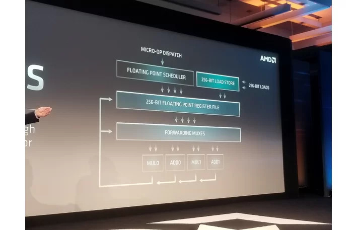
According to Expreview, AMD conducted DKERN + RSA test for integer and floating point units, to arrive at a performance index of 4.53, compared to 3.5 of first-generation Zen, which is a 29.4 percent IPC uplift (loosely interchangeable with single-core performance). "Zen 2" goes a step beyond "Zen+," with its designers turning their attention to critical components that contribute significantly toward IPC - the core's front-end, and the number-crunching machinery, FPU. The front-end of "Zen" and "Zen+" cores are believed to be refinements of previous-generation architectures such as "Excavator." Zen 2 gets a brand-new front-end that's better optimized to distribute and collect workloads between the various on-die components of the core. The number-crunching machinery gets bolstered by 256-bit FPUs, and generally wider execution pipelines and windows. These come together yielding the IPC uplift. "Zen 2" will get its first commercial outing with AMD's 2nd generation EPYC "Rome" 64-core enterprise processors.

Update Nov 14: AMD has issued the following statement regarding these claims.
As we demonstrated at our Next Horizon event last week, our next-generation AMD EPYC server processor based on the new 'Zen 2' core delivers significant performance improvements as a result of both architectural advances and 7nm process technology. Some news media interpreted a 'Zen 2' comment in the press release footnotes to be a specific IPC uplift claim. The data in the footnote represented the performance improvement in a microbenchmark for a specific financial services workload which benefits from both integer and floating point performance improvements and is not intended to quantify the IPC increase a user should expect to see across a wide range of applications. We will provide additional details on 'Zen 2' IPC improvements, and more importantly how the combination of our next-generation architecture and advanced 7nm process technology deliver more performance per socket, when the products launch.
Source: Expreview
Add your own comment

162 Comments on AMD "Zen 2" IPC 29 Percent Higher than "Zen"

#51
HD64G
ValantarWhile you're right that we don't know yet that the CCXes have grown to 8 cores (though IMO this seems likely given that every other Zen2 rumor has been spot on), that drawing is ... nonsense. First off, it proposes using IF to communicate between CCXes on the same die, which even Zen1 didn't do. The sketch directly contradicts what AMD said about their design, and doesn't at all account for the I/O die and its role in inter-chiplet communication. The layout sketched out there is incredibly complicated, and wouldn't even make sense for a theoretical Zen1-based 8-die layout. Remember, IF uses PCIe links, and even in Zen1 the PCIe links were common across two CCXes. The CCXes do thus not have separate IF links, but share a common connection (through the L3 cache, IIRC) to the PCIe/IF complex. Making these separate would be a giant step backwards in terms of design and efficiency. Remember, the uncore part of even a 2-die Threadripper consumes ~60W. And that's with two internal links, 64 lanes of PCIe and a quad-channel memory controller. The layout in the sketch above would likely consume >200W for IF alone.

Now, let's look at that sketch. In it, any given CCX is one hop away from 3-4 other CCXes, 2 hops from 3-5 CCXes, and 3 hops away from the remaining 7-10 CCXes. In comparison, with EPYC (non-Rome) and TR, all cores are 1 hop away from each other (though the inter-CCX hop is shorter/faster than the die-to-die IF hop). Even if this is "reduced latency IF" as they call it, that would be ridiculous. And again: what role does the I/O die play in this? The IF layout in that sketch makes no use of it whatsoever, other than linking the memory controller and PCIe lanes to eight seemingly random CCXes. This would make NUMA management an impossible flustercuck on the software side, and substrate manufacturing (seriously, there are six IF links in between each chiplet there! The chiplets are <100mm2! This is a PCB, not an interposer! You can't get that kind of trace density in a PCB.) impossible on the hardware side. Then there's the issue of this design requiring each CCX to have 4 IF links, but 1/4 of the CCXes only gets to use 3 links, wasting die area.

On the other hand, let's look at the layout that makes sense both logically, hardware and software wise, and adds up with what AMD has said about EPYC: Each chiplet has a single IF interface, that connects to the I/O die. Only that, nothing more. The I/O die has a ring bus or similar interconnect that encompasses the 8 necessary IF links for the chiplets, an additional 8 for PCIe/external IF, and the memory controllers. This reduces the number of IF links running through the substrate from 30 in your sketch (6 per chiplet pair + 6 between them) to 8. It is blatantly obvious that the I/O die has been made specifically to make this possible. This would make every single core 1 hop (through the I/O die, but ultimately still 1 hop) away from any other core, while reducing the number of IF links by almot 1/4. Why else would they design that massive die?

Red lines. The I/O die handles low-latency shuffling of data between IF links, while also giving each chiplet "direct" access to DRAM and PCIe. All over the same single connection per chiplet. The I/O die is (at least at this time) a black box, so we don't know whether it uses some sort of ring bus, mesh topology, or large L4 cache (or some other solution) to connect these various components. But we do know that a layout like this is the only one that would actually work. (And yes, I know that my lines don't add up in terms of where the IF link is physically located on the chiplets. This is an illustration, not a technical drawing.)

More on-topic, we need to remember that IPC is workload dependent. There might be a 29% increase in IPC in certain workloads, but generally, when we talk about IPC it is average IPC across a wide selection of workloads. This also applies when running test suites like SPEC or GeekBench, as they run a wide variety of tests stressing various parts of the core. What AMD has "presented" (it was in a footnote, it's not like they're using this for marketing) is from two specific workloads. This means that a) this can very likely be true, particularly if the workloads are FP-heavy, and b) this is very likely not representative of total average IPC across most end-user-relevant test suites. In other words, this can be both true (in the specific scenarios in question) and misleading (if read as "average IPC over a broad range of workloads").
Agreed. Interesting graph but and I also think it has mistakes. AMD put this central die in the middle of the chiplets to allow all of them be as close as possible to it. And they put the memory controller there also to cancel the need of those chiplets to communicate at all. The CPU will use as many cores as needed by the sw and use the IO chip to do the rest. And that is why imho this arch is brilliant and the only way to increase core count without increase latency to the moon. We are warching a true revolution in computing here. My 5 cents.
Posted on Reply
#52
bug
Vayra86Eh... IPS in my mind is In Plane Switching for displays.

He spelled it fine, you didn't read it right.
Happens to me too from time to time. Especially when I read or post in a hurry.
Posted on Reply
#53
Markosz
Oh, investor meeting... then let's take half of what they said
Posted on Reply
#54
Valantar
Smartcom5Excuse me sir, but you misspelled IPS! When people will finally learn the difference ffs?!
Vayra86Eh... IPS in my mind is In Plane Switching for displays.

He spelled it fine, you didn't read it right.
Agreed. There's nothing wrong with saying "Intel has a clock speed advantage, but AMD might beat them in actual performance through increasing IPC." There's nothing in that saying that clock speed affects IPC, only that clock speed is a factor in actual performance. Which it is. What @Smartcom5 is calling "IPS" is just actual performance (which occurs in the real world, and thus includes time as a factor, and thus also clock speed) and not the intentional abstraction that IPC is. This seems like a fundamental misunderstanding of why we use the term IPC in the first place (to separate performance from the previous misunderstood oversimplification that was "faster clocks=more performance").
Posted on Reply
#55
Dante Uchiha
btarunrThere are two ways AMD could built a 16-core AM4 processor:
  • Two 8-core chiplets with a smaller I/O die that has 2-channel memory, 32-lane PCIe gen 4.0 (with external redrivers), and the same I/O as current AM4 dies such as ZP or PiR.
  • A monolithic die with two 8-core CCX's, and fully integrated chipset like ZP or PiR. Such a die wouldn't be any bigger than today's PiR.
I think option two is more feasible for low-margin AM4 products.
That's not realistic. 16c is not feasible for consumers:

-16c with high clocks would have a high TDP, the current motherboards would have been problems to support them.
-16c would have to be double the current value of the 2700x, and even then AMD would have a lower profit/cpu sold.
- 8c CPU is more than enough for gaming, even for future releases.

Would you buy a 3700x @ 16c at U$ 599~ ? Or would be better a 3700x with "just 8c", low latency, optimized for gaming at U$ 349~399 ?
Posted on Reply
#56
R0H1T
We're not getting 32 PCIe 4.0 lanes on AM4, I'd be (really) shocked if that were the case.

Valantar with the entire I/O & MC off the die it opens up a world of possibilities with Zen, having said that I'll go back again to the point I made in other threads. The 8 core CCX makes sense for servers & perhaps HEDT, however when it comes to APU (mainly notebooks) I don't see a market for 8 cores there. I also don't see AMD selling an APU with 6/4 cores disabled, even if it is high end desktop/notebooks.

The point I'm making is that either AMD makes two CCX, one with 8 cores & the other with 4, or they'll probably go with the same 4 core CCX. The image I posted is probably misconstrued, I also don't know for certain if the link shown inside the die is IF or just a logical connection (via L3?) between 2 CCX.
Posted on Reply
#57
Valantar
HD64GInteresting graph but I think it has mistakes. AMD put this central die in the middle of the chiplets to allow all of them be as close as possible to it. And they put the memory controller there also to cancel the need of those chiplets to communicate at all. The CPU will use as many cores as needed by the sw and use the IO chip to do the rest. And that is why imho this arch is brilliant and the only way to increase core count without increase latency to the moon. We are warching a true revolution in computing here. My 5 cents.
You're phrasing this as if you're arguing against me, yet what you're saying is exactly what I'm saying. Sounds like you're replying to the wrong post. The image I co-opted came from the quoted post, I just sketched in how I believe they'll lay this out.
Posted on Reply
#58
TheinsanegamerN
If AMD managed a 15% IPC increase over OG zen, I would be amazed. I was expecting around 10%.

There is no way they will hit 20-29%. That is just wishful thinking on AMD's part, most likely in specific scenarios.

Of course, I'd love to e proved wrong here.
Posted on Reply
#59
Valantar
R0H1TWe're not getting 32 PCIe 4.0 lanes on AM4, I'd be (really) shocked if that were the case.

Valantar with the entire I/O & MC off the die it opens up a world of possibilities with Zen, having said that I'll go back again to the point I made in other threads. The 8 core CCX makes sense for servers & perhaps HEDT, however when it comes to APU (mainly notebooks) I don't see a market for 8 cores there. I also don't see AMD selling an APU with 6/4/2 cores disabled, even if it is high end desktop/notebooks.

The point I'm making is that either AMD makes two CCX, one with 8 cores & the other with 4, or they'll probably go with the same 4 core CCX. The image I posted is probably misconstrued, I also don't know for certain if the link shown inside the die is IF or just a logical connection between 2 CCX.
I partially agree with that - it's very likely they'll put out a low-power 4-ish-core chiplet for mobile. After all, the mobile market is bigger than the desktop market, so it makes more sense for this to get bespoke silicon. What I disagree with is the need for the 8-core to be based off the same CCX as the 4-core. If they can make an 8-core CCX, equalising latencies between cores on the same die, don't you think they'd do so? I do, as that IMO qualifies as "low-hanging fruit" in terms of increasing performance from Zen/Zen+. This would have performance benefits for every single SKU outside of the mobile market. And, generally, it makes sense to assume that scaling down core count per CCX is no problem, so having an 8-core version is no hindrance to also having a 4-core version.

How I envision AMD's Zen2 roadmap:

Ryzen Mobile:
15-25W: 4-core chiplet + small I/O die (<16 lanes PCIe, DC memory, 1-2 IF links), either integrated GPU on the chiplet or separate iGPU chiplet
35-65W: 8-core chiplet + small I/O die (<16 lanes PCIe, DC memory, 1-2 IF links), separate iGPU chiplet or no iGPU (unlikely, iGPU useful for power savings)

Ryzen Desktop:
Low-end: 4-core chiplet + medium I/O die (< 32 lanes PCIe, DC memory, 2 IF links), possible iGPU (either on-chiplet or separate)
Mid-range: 8-core chiplet + medium I/O die (< 32 lanes PCIe, DC memory, 2 IF links), possible iGPU on specialized SKUs
High-end: 2x 8-core chiplet + medium I/O die (< 32 lanes PCIe, DC memory, 2 IF links)

Threadripper:
(possible "entry TR3": 2x 8-core chiplet + large I/O die (64 lanes PCIe, QC memory, 4 IF links), though this would partially compete with high-end Ryzen just with more RAM B/W and PCIe and likely only have a single 16-core SKU, making it unlikely to exist)
Main: 4x 8-core chiplet + large I/O die (64 lanes PCIe, QC memory, 4 IF links)

EPYC:
Small: 4x 8-core chiplet + XL I/O die (128 lanes PCIe, 8C memory, 8 IF links)
Large: 8x 8-core chiplet + XL I/O die (128 lanes PCIe, 8C memory, 8 IF links)

Uncertiainty:
-Mobile might go with an on-chiplet iGPU and only one IF link on the I/O die, but this would mean no iGPU on >4-core mobile SKUs (unless they make a third chiplet design), while Intel already has 6-cores with iGPUs. As such, I'm leaning towards 2 IF links and a separate iGPU chiplet for ease of scaling, even if the I/O die will be slightly bigger and IF power draw will increase.

Laying out the roadmap like this has a few benefits:
-Only two chiplet designs across all markets.
-Scaling happens through I/O dice, which are made on an older process, are much simpler than CPUs, and should thus be both quick and cheap to make various versions of.
-A separate iGPU chiplet connected through IF makes mobile SKUs easier to design, and the GPU die might be used in dGPUs also.
-Separate iGPU chiplets allow for multiple iGPU sizes - allowing more performance on the high end, or less power draw on the low end.
-Allows for up to 8-core chips with iGPUs in both mobile and desktop.

Of course, this is all pulled straight out of my rear end. Still, one is allowed to dream, no?
TheinsanegamerNIf AMD managed a 15% IPC increase over OG zen, I would be amazed. I was expecting around 10%.

There is no way they will hit 20-29%. That is just wishful thinking on AMD's part, most likely in specific scenarios.

Of course, I'd love to e proved wrong here.
Well, they claim to have measured a 29.4% increase. That's not wishful thinking at least. But as I pointed out in a previous post:
ValantarWe need to remember that IPC is workload dependent. There might be a 29% increase in IPC in certain workloads, but generally, when we talk about IPC it is average IPC across a wide selection of workloads. This also applies when running test suites like SPEC or GeekBench, as they run a wide variety of tests stressing various parts of the core. What AMD has "presented" (it was in a footnote, it's not like they're using this for marketing) is from two specific workloads. This means that a) this can very likely be true, particularly if the workloads are FP-heavy, and b) this is very likely not representative of total average IPC across most end-user-relevant test suites. In other words, this can be both true (in the specific scenarios in question) and misleading (if read as "average IPC over a broad range of workloads").
Posted on Reply
#60
TheinsanegamerN
ValantarWell, they claim to have measured a 29.4% increase. That's not wishful thinking at least. But as I pointed out in a previous post:
AMD also "claimed" to have dramatically faster CPUs with bulldozer, and "claimed" Vega would be dramatically faster then it ended up being. AMD here "claims" to have measured a 29.4% increase in IPC. But that might have been in a workload that uses AVX, and is heavily threaded, or somehow built to take full advantage of ryzen.

I'll wait for third party benchmarks. AMD has made way too many *technically true claims over the years.

*Technically true in one specific workload, overall the performance boost was less then half what AMD claimed, but it was true in one workload, so technically they didnt lie.
Posted on Reply
#61
Vya Domus
randomUserIf you your task requires 1000 instructions to be completed, then:
Zen1 will finish this task in 1000 clock cycles;
Zen2 will finish this task in 775 clock cycles.
That's not how this works, not all instruction see the same improvement.
TheinsanegamerNI'll wait for third party benchmarks. AMD, Intel, Nvidia have made way too many *technically true claims over the years.
Fixed it.
Posted on Reply
#62
GlacierNine
ValantarI partially agree with that - it's very likely they'll put out a low-power 4-ish-core chiplet for mobile. After all, the mobile market is bigger than the desktop market, so it makes more sense for this to get bespoke silicon. What I disagree with is the need for the 8-core to be based off the same CCX as the 4-core. If they can make an 8-core CCX, equalising latencies between cores on the same die, don't you think they'd do so? I do, as that IMO qualifies as "low-hanging fruit" in terms of increasing performance from Zen/Zen+. This would have performance benefits for every single SKU outside of the mobile market. And, generally, it makes sense to assume that scaling down core count per CCX is no problem, so having an 8-core version is no hindrance to also having a 4-core version.
I disagree, for one very simple reason - Tooling up production for 2 different physical products/dies would likely be more expensive than the material savings in not using as much silicon per product. This stuff is not cheap to do, and in CPU manufacture, volume savings are almost always much more dramatic than design/material savings.

Serving Mainstream, HEDT, and Server customers from a single die integrated into multiple packages, is one of the main reasons AMD are in such good shape right now - Intel has to produce their Mainstream, LCC, HCC, and XCC dies and then bin and disable cores on all 4 of them for each market segment. AMD only has to produce and bin one die, to throw onto a variety of packages at *every level* of their product stack.

It's not even worth producing a second die unless the move would bring in not only more profit, but enough extra profit to completely cover the cost of tooling up for that. Bear in mind here that I mean something very specific:

If AMD spends 1bn to produce a second die, and rakes in 1.5bn extra profit over last year, that doesn't necessarily mean tooling up for the extra die was worth it. What if their profits still would have gone up by 1bn anyway, using a single die in production? If that were the case, tooling up just cost AMD a cool $1,000,000,000 in order to make $500,000,000. Sure, they might have gained a bit more marketshare, but not only did it lose them money, it also ended up making their product design procedures more complex and caused additional overheads right the way up through every level of the company, keeping track of the two independent pieces of silicon. It also probably means having further stratification in motherboards and chipsets, whereas right now AMD are very flexible in what they can do to bring these packages to older chipsets or avoid bringing in new ones.

Edit: Not to mention, that using a single, much higher capability die, has other benefits - Like for example being able to provide customers with a *much* longer support period for upgrades - something that has already won them sales with their "AM4 until 2020" approach bringing in consumers who are sick of Intel's socket and chipset-hopping.

Or simply being able to unlock CCXs on new products as and when the market demands that - After all, why would you intentionally design a product that reduces your ability to respond to competition, when your competition is Intel, who you *know* are scrambling to use their higher R&D budget to smack you down again before you get too far ahead?
Posted on Reply
#63
dirtyferret
I could "potentially" be making 29% more money next year if the company owner doesn't get in the way.
Posted on Reply
#64
B-Real
Prima.VeraBulldozer, Excavator, ... no thank you. No more hyping until the community benches are out. :rolleyes:
You will see this after they are released. :) Even if there will be only a ~10% increase from Zen+, they will be on par with Intel in FHD games tested with a 2080Ti.
Posted on Reply
#65
GlacierNine
bug95W+ or scarcity are not new to the mainstream market ;)
Even the price is not that out of this world, but at $500 it won't gain 10% market share, so yeah, not that mainstream after all.
"95W+" is a bit misleading. Nobody should be looking at the 9900K and pretending it's simply a return to the hotter chips of yore. The fact is, it's actually a dramatically hotter chip than almost anything that has come before it, and the only reason we're able to tame it is because the coolers we use these days are so much more capable. At the time we were dealing with Intel Prescott chips, one of the best coolers you could buy was the Zalman CNPS9500. Noctua were only just about to release the *first* NH-U12. The undisputed king of the hill for air cooling was the Tuniq Tower 120, soon to be displaced by the original Thermalright Ultra 120.

The NH-D15 didn't exist. There were no AIOs of any kind, and that's why back then, we all struggled to cool Prescott Cores and first Gen i7s.

For example, The i7 975 was a 130W part. The fastest Pentium 4 chips were officially 115W. Intel's Datasheets of that time don't specify how TDP was calculated, but if we assume that they were doing what they do now, which is quote TDP at base clocks under a "close to worst case" workload, then we're probably in good shape.

The i7-975 then, had a 3,333MHz base clock, a 3.467 All-Core boost, and a 3.6GHz single core boost. Not a lot of boost happening here, only an extra 133MHz on all cores. You'd expect no real increase in temperatures under your cooler from such a mild overclock, unless you were OC'ing something like an old P3, so we can probably assume that means the Intel TDP from then, if measured according to today's standards, was probably pretty close to "correct" - You could expect your i7 975 to stick pretty close to that 130W TDP figure in a real world scenario. And this was legitimately a hard to cool chip! Even the best air coolers sometimes struggled.

Compare that to the 9900K, which is breaking 150W power consumption all over the internet, and you suddenly realise - The only reason these chips are surviving in the wild is because:

1 - Intel's current Arch will maintain it's maximum clocks way up into the 90+ Celsius range
2 - People are putting them under NH-D15s - and even then we're seeing temperature numbers that, back in the P4 days, would have been considered "Uncomfortable" and "dangerous".

The 9900K is, as far as I can tell, simply the most power hungry and hard to cool processor that Intel has ever released on a mainstream platform. It runs at the *ragged edge* of acceptability. You can't just brush this sort of thing off with "The market has seen 95W chips before". That's not what the 9900K actually is. It's something much, much more obscene.
Posted on Reply
#66
Smartcom5
bugNo, I meant just what I said/wrote ;)
Gosh, I'm really sorry, was my bad!
Picked the wrong quote, was meant to quote @WikiFM
WikiFM… I thought Zen was still way behind Intel in single threaded performance or IPC.
Smartcom
Posted on Reply
#67
bug
GlacierNine"95W+" is a bit misleading. Nobody should be looking at the 9900K and pretending it's simply a return to the hotter chips of yore. The fact is, it's actually a dramatically hotter chip than almost anything that has come before it, and the only reason we're able to tame it is because the coolers we use these days are so much more capable. At the time we were dealing with Intel Prescott chips, one of the best coolers you could buy was the Zalman CNPS9500. Noctua were only just about to release the *first* NH-U12. The undisputed king of the hill for air cooling was the Tuniq Tower 120, soon to be displaced by the original Thermalright Ultra 120.
That is completely wrong. 9900k is a 95W chip and will work within a 95W power envelope. It has potential to work faster when unconstrained, but it will work with a 95W heat sink. Old Pentium Ds were 130W chips and back then, Intel's guidance was only for average power draw, not maximal (kind of like those 95W mean today, though not exactly the same).
That said, there's no denying what Intel has now is redesign trying to fit more tricks into the current process node which should be long behind us. Thus, it's an architecture stretched past its intended lifetime.
Posted on Reply
#68
Smartcom5
ValantarWhat @Smartcom5 is calling "IPS" is just actual performance (which occurs in the real world, and thus includes time as a factor, and thus also clock speed) and not the intentional abstraction that IPC is.
I'm sorry but I'm not just 'calling' it as such, I just pointed out how things are actually standardised. IPC, IPS and CPI in fact are known and common figures, hence the wiki-links. But as you can see, the whole thing isn't as nearly as trivial as it might look to be.

That's why actual Performance is usually by default measured using the figure of the actually absolute and fixed unit FLOPS (Floating Point Operations Per Second) or MIPS (Million Instructions per Second) – hence the performance of instructions per (clock-) cycle while performing a processing of a equally pre-defined kind of instruction (in this case, floating-point numbers).


Smartcom
Posted on Reply
#69
HD64G
ValantarYou're phrasing this as if you're arguing against me, yet what you're saying is exactly what I'm saying. Sounds like you're replying to the wrong post. The image I co-opted came from the quoted post, I just sketched in how I believe they'll lay this out.
My mistake indeed and I edited my post to correct the misunderstanding. Cheers! :toast:
Posted on Reply
#70
GlacierNine
bugThat is completely wrong. 9900k is a 95W chip and will work within a 95W power envelope. It has potential to work faster when unconstrained, but it will work with a 95W heat sink. Old Pentium Ds were 130W chips and back then, Intel's guidance was only for average power draw, not maximal (kind of like those 95W mean today, though not exactly the same).
That said, there's no denying what Intel has now is redesign trying to fit more tricks into the current process node which should be long behind us. Thus, it's an architecture stretched past its intended lifetime.
Oh please, stop the apologism. The 9900K will work within a 95W power envelope, yes. At 3.6GHz base clock, with occasional jumps to higher speeds where the cooling solution's "thermal capacitance" can be leveraged.

But these chips and this silicon aren't designed to be 3.6GHz parts in daily use. They are ~4.7GHz parts that Intel reduced the base clocks on, in order to be able to claim a 95W TDP. If you had the choice between running a 7700K and a 9900K at base clocks, the 7700K would actually get you the better gaming performance in most games. Would you say that's Intel's intention? To create a market where a CPU 2 generations old, with half the cores, outperforms their current flagship in exactly the task Intel advertise the 9900K to perform?

Or would you say that actually, Intel has transitioned from using boost clock as "This is extra performance if you can cool it", to using boost clock as the figure expected to sell the CPU, and therefore the figure most users expect to see in use?

You can clearly see this in the progression of the flagships, each generation.

6700K - 4.0GHz Base, 4 Cores, 95W TDP
7700K - 4.2GHz Base, 4 Cores, 95W TDP
8700K - 3.7GHz Base, 6 Cores, 95W TDP
9900K - 3.6GHz Base, 8 Cores, 95W TDP.

Oh well would you look at that - As soon as Intel started adding cores, they dropped the base clocks dramatically in order to keep their "95W TDP at base clocks" claim technically true. But look at the all core boost clocks:

4.0GHz, 4.4GHz, 4.3GHz, 4.7GHz

They dipped by 100MHz on the 8700K, to prevent a problem similar to the 7700K, which was known to spike in temperature even under adequate cooling, only to come back up on the 9900K, but this time with Solder TIM to prevent that from happening.

Single core is the same story - 4.2, 4.5, 4.7, 5.0. A constant increase in clockspeed each generation.

Like I said - Boost is no longer a boost. Boost has become the expected performance standard of Intel chips. Once you judge the chips on that basis, the 9900K reveals itself to be a power hungry monster that makes the hottest Prescott P4 chips look mild in comparison.
Posted on Reply
#71
bug
GlacierNineThe 9900K will work within a 95W power envelope, yes. At 3.6GHz base clock, with occasional jumps to higher speeds where the cooling solution's "thermal capacitance" can be leveraged.
Oh please, stop the apologism. These chips aren't 95W, 3.6GHz parts that Intel have magically made capable of overclocking themselves by 1.1GHz on all cores. They are ~4.7GHz parts that Intel reduced the base clocks on, in order to be able to claim a 95W TDP. If you could go back in time and cast a magic spell that

You can clearly see this in the progression of the flagships, each generation.

6700K - 4.0GHz Base, 4 Cores, 95W TDP
7700K - 4.2GHz Base, 4 Cores, 95W TDP
8700K - 3.7GHz Base, 6 Cores, 95W TDP
9900K - 3.6GHz Base, 8 Cores, 95W TDP.

Oh well would you look at that - As soon as Intel started adding cores, they dropped the base clocks dramatically in order to keep their "95W TDP at base clocks" claim technically true. But look at the all core boost clocks:

4.0GHz, 4.4GHz, 4.3GHz, 4.7GHz

They dipped by 100MHz on the 8700K, to prevent a problem similar to the 7700K, which was known to spike in temperature even under adequate cooling, only to come back up on the 9900K, but this time with Solder TIM to prevent that from happening.

Single core is the same story - 4.2, 4.5, 4.7, 5.0. A constant increase in clockspeed each generation.

Intel's game here has been to transition from "Intel Turbo Boost Technology allows your processor to go beyond base specs" as their marketing angle, to a standpoint of "If your cooling can't allow the chip to boost constantly, then you're wasting the potential of your CPU". It's not even wrong - you *are* wasting the potential of your extremely expensive CPU if you don't manage to run it *WELL* into boost clock these days.
I'm not sure where you and I disagree. All these CPUs will work at 95W at their designated baseline clocks. With beefier heat sinks you can extract more performance. Nothing has changed, except the boost algorithms that have become smarter. Would you prefer a hard 95W limitation instead or what's your beef here?
Posted on Reply
#72
efikkan
It seems to me like this article is based on a bad translation referring to a 29% performance uplift (partially due to increased FPU width). For starters, to estimate IPC the clock speed would have to be at completely fixed (no boost). Secondly, in reality performance is not quite as simple as clock times "IPC", due to memory latency becoming a larger bottleneck with higher clocks.

A 29% IPC uplift would certainly be welcome, but keep in mind this is about twice the accumulated improvements from Sandy Bridge -> Skylake. I wonder how this thread would turn out if someone claimed Ice Lake would offer 29% IPC gains?:rolleyes:
Let's not have another Vega Victory Dance™. We need to clam down this extreme hype and be realistic. Zen 2 is an evolved Zen, it will probably do tweaks and small improvements across the design, but it will not be a major improvement over Zen.
Posted on Reply
#74
R0H1T
GlacierNineI disagree, for one very simple reason - Tooling up production for 2 different physical products/dies would likely be more expensive than the material savings in not using as much silicon per product. This stuff is not cheap to do, and in CPU manufacture, volume savings are almost always much more dramatic than design/material savings.

Serving Mainstream, HEDT, and Server customers from a single die integrated into multiple packages, is one of the main reasons AMD are in such good shape right now - Intel has to produce their Mainstream, LCC, HCC, and XCC dies and then bin and disable cores on all 4 of them for each market segment. AMD only has to produce and bin one die, to throw onto a variety of packages at *every level* of their product stack.

It's not even worth producing a second die unless the move would bring in not only more profit, but enough extra profit to completely cover the cost of tooling up for that. Bear in mind here that I mean something very specific:

If AMD spends 1bn to produce a second die, and rakes in 1.5bn extra profit over last year, that doesn't necessarily mean tooling up for the extra die was worth it. What if their profits still would have gone up by 1bn anyway, using a single die in production? If that were the case, tooling up just cost AMD a cool $1,000,000,000 in order to make $500,000,000. Sure, they might have gained a bit more marketshare, but not only did it lose them money, it also ended up making their product design procedures more complex and caused additional overheads right the way up through every level of the company, keeping track of the two independent pieces of silicon. It also probably means having further stratification in motherboards and chipsets, whereas right now AMD are very flexible in what they can do to bring these packages to older chipsets or avoid bringing in new ones.

Edit: Not to mention, that using a single, much higher capability die, has other benefits - Like for example being able to provide customers with a *much* longer support period for upgrades - something that has already won them sales with their "AM4 until 2020" approach bringing in consumers who are sick of Intel's socket and chipset-hopping.

Or simply being able to unlock CCXs on new products as and when the market demands that - After all, why would you intentionally design a product that reduces your ability to respond to competition, when your competition is Intel, who you *know* are scrambling to use their higher R&D budget to smack you down again before you get too far ahead?
The market (retail?) you're talking about is also huge, in fact bigger than enterprise even for Intel.
If the (extra) power savings materialize for ULP & ULV products then it makes sense to deploy a 4 core CCX over there, however an 8 core CCX will have better latencies & probably higher clocks as well.
bugI'm not sure where you and I disagree. All these CPUs will work at 95W at their designated baseline clocks. With beefier heat sinks you can extract more performance. Nothing has changed, except the boost algorithms that have become smarter. Would you prefer a hard 95W limitation instead or what's your beef here?
Fake 95W TDP?
Posted on Reply
#75
GlacierNine
bugI'm not sure where you and I disagree. All these CPUs will work at 95W at their designated baseline clocks. With beefier heat sinks you can extract more performance. Nothing has changed, except the boost algorithms that have become smarter. Would you prefer a hard 95W limitation instead or what's your beef here?
Smarter boost algorithms have absolutely nothing to do with this. Intel already had Speedstep to take care of dynamically downclocking the CPU to lower power states during low-intensity workloads In fact they've had it since 2005, so long that their trademark on Speedstep lapsed in 2012.

My 6700K has no trouble downclocking to save power when it's not necessary. The 3rd Gen i5 I'm typing this on has no trouble with that either. The Pentium 4 660 had it, I can find from a cursory google. In fact, support for the power-saving tech was originally mainly difficult not due to the platforms, but because of a lack of operating system support for the feature. "Smarter" power saving algorithms should have nothing to do with "Turbo boost" technology.

We disagree in that you think it is reasonable for Intel to consider a 9900K as "working according to spec" at 3.6GHz and "Overclocked" at 4.7GHz, when clearly these products are actually designed to run at higher clocks, and are expected to by consumers, and *will run* at higher clocks, it's just that it is only achievable at a *much* higher TDP than intel claims their CPU actually has.

They can't have their cake and eat it - Either the 9900K is "The world's fastest gaming CPU (At 150W TDP)", or it is a 95W part (but isn't anywhere close to being the fastest gaming CPU at that TDP).

Intel should not be allowed to advertise this product as both of these mutually exclusive things.
Posted on Reply
Add your own comment
Apr 24th, 2024 21:12 EDT change timezone

New Forum Posts

Popular Reviews

Controversial News Posts