Wednesday, July 3rd 2019

NVIDIA Manufacturing Turing GPUs at Samsung Korea Fab, 11nm?

During our disassembly of the GeForce RTX 2060 Super, we noticed a shocking detail. The 12 nm "TU106" GPU on which it is based, has the marking "Korea." We know for a fact that TSMC does not have any fabs there. The only Korean semiconductor manufacturer capable of contract-manufacturing a piece of silicon as complex as a GPU, for a designer with the energy-efficiency OCD as NVIDIA, is Samsung.

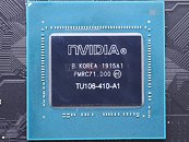
What makes this interesting is that Samsung does not officially have a 12 nm FinFET process. It has 14 nm, and the 11LPP, a 11 nm nodelet, which the company designed to compete with TSMC 12 nm. It would hence be really interesting to hear from NVIDIA on whether they've scaled out the "TU106" to 14LPP, or down to 11LPP at Samsung. It's interesting to note that the shrink in transistor sizes in these nodelets doesn't affect die-sizes. We hence see no die-size difference between these Korea-marked chips, and those marked "Taiwan." We've reached out to NVIDIA for comment.

Update July 3rd: NVIDIA got back to us
NVIDIAThe answer is really simple and these markings are not new. Other Turing GPUs have had these markings in the past. The chip is made at TSMC, but packaged in various locations. This one was done in Korea, hence why his says "Korea".

On an unrelated note: We already use both TSMC and Samsung, and qualify each of them for every process node. We can't comment in any further detail on future plans, but both remain terrific partners.
Add your own comment

33 Comments on NVIDIA Manufacturing Turing GPUs at Samsung Korea Fab, 11nm?

#1
EarthDog
It would be nice to know what NVIDIA said to complete this news piece instead of a teaser...
Posted on Reply
#2
jabbadap
All chips comes from TSMC 12nm FFN node. That etching is marking where packaging has been made(Korea or Taiwan). I.E. gp107 samsung chip cards are usually packaged in Taiwan.
Posted on Reply
#3
ppn
20-series were originally designed for Samsung 8LPP but nvidia left the door open for 11LPP. must be 11 with 9T library same as 14LPP. that is why no die size benefits, just power and clock. So there is no 8LPP and we can hope for 7nm EUV in 2020.
Posted on Reply
#4
jeremyshaw
jabbadapAll chips comes from TSMC 12nm FFN node. That etching is marking where packaging has been made(Korea or Taiwan). I.E. gp107 samsung chip cards are usually packaged in Taiwan.
Those may be packaged in Taiwan, but all the ones I've seen are still marked with Korea.

EDIT: I see the link. Nice, I haven't seen those before.
Posted on Reply
#6
R-T-B
VulcansheartSo, is this fake news, or....
Since they've backed away from making any hard claims, no, it's not "fake news."

It is kind of sensationalist though.
Posted on Reply
#7
Fatalfury
I hope next generation gpu Turing refresh/ampere due to release 2020 will be 7nm and not 11nm.. If amd 7nm is not good enough.. Nvidia can delay 7nm and still go with 11nm for RTX 3000 series
Posted on Reply
#8
Mephis
R-T-BSince they've backed away from making any hard claims, no, it's not "fake news."

It is kind of sensationalist though.
Of course it is sensationalist, look who wrote it. I mean the responsible thing to do would have been to not post anything until he heard from Nvidia, but then there wouldn't have been a "possible" story.
Posted on Reply
#9
bug
MephisOf course it is sensationalist, look who wrote it. I mean the responsible thing to do would have been to not post anything until he heard from Nvidia, but then there wouldn't have been a "possible" story.
I don't get what could be sensational about this. Samsung's 11nm is identical for all intents and purposes to TSMC's 12nm, there would be no competitive advantage to be had here.
Posted on Reply
#10
EarthDog
So, this was updated, thank you!

Is it just me or does that response make this 'news' article look like a reach (at best). Instead of keeping the foot close to the mouth for insertion by getting 'news' out there, why not get the answer first? I'd rather have not seen this speculation come up only to be bunked a day later.
Posted on Reply
#11
bug
EarthDogSo, this was updated, thank you!

Is it just me or does that response make this 'news' article look like a reach (at best). Instead of keeping the foot close to the mouth for insertion by getting 'news' out there, why not get the answer first? I'd rather have not seen this speculation come up only to be bunked a day later.
There's no smoke without fire.
Nvidia says TSMC, TSMC makes chips in Taiwan, GPU says Korea. It was noteworthy. At least now we have all learned TSMC packages chips in Korea :P
Posted on Reply
#12
IceShroom
Well Vega and Polaris chips are fabed in USA, but has Made in Taiwan as those are packaged in Taiwan. Maybe Nvidia fabing those chip in Taiwan and packaging in Korea, like AMD.
Posted on Reply
#13
iO
Same die size was a dead giveaway that its not made on a different process node.
GPU markings denote location of packaging not manufacturing. Like the Samsung-made GP107 had Taiwan written on it.
Posted on Reply
#14
Mephis
bugI don't get what could be sensational about this. Samsung's 11nm is identical for all intents and purposes to TSMC's 12nm, there would be no competitive advantage to be had here.
Its sensationalist in the fact that he had no evidence for the story. It's not like he had a source that said Nvidia switched to Samsung. All he had was a marking on a chip, a marking that he didn't know what it meant. So he reached out to Nvidia, which was the right and proper step. He should have waited for their response. Instead he published a story, based only on something that he came up with.
Posted on Reply
#15
bug
iOSame die size was a dead giveaway that its not made on a different process node.
GPU markings denote location of packaging not manufacturing. Like the Samsung-made GP107 had Taiwan written on it.
12nm -> 11nm will not yield a different die size ;)
MephisIts sensationalist in the fact that he had no evidence for the story. It's not like he had a source that said Nvidia switched to Samsung. All he had was a marking on a chip, a marking that he didn't know what it meant. So he reached out to Nvidia, which was the right and proper step. He should have waited for their response. Instead he published a story, based only on something that he came up with.
He said he didn't have further evidence and that he's contacted Nvidia and waiting for a response.

Edit: Not every tech news has to be about groundbreaking stuff, sometimes it's about little things/smalltalk.
Posted on Reply
#16
EarthDog
I wonder of W1z, the GPU guru of TPU was consulted before publishing. If anyone here knew....
Posted on Reply
#17
iO
bug12nm -> 11nm will not yield a different die size ;)
Yea thats not how it works.
Edit: Even when the size could be similar, there wouldn't be the exact same capacitor placement around the chip.
Posted on Reply
#18
bug
iOYea thats not how it works.
Edit: Even when the size could be similar, there wouldn't be the exact same capacitor placement around the chip.
I see. You must be one of those thinking a transistor made on 11nm tech is a square/cube with a 11nm side.
Posted on Reply
#19
ironcerealbox
EarthDogIt would be nice to know what NVIDIA said to complete this news piece instead of a teaser...
Yeah, there's a great movie titled "The Paper" and y'know, it's basics about writing any news. Get the facts straight and only then, print. It started with sensationalist headlines and then went to sensationalism. It migrated to broadcast journalism and now it's migrated to social media and the internet news.
Posted on Reply
#20
EarthDog
Some strive to rise above... others, not so much. It's a click bait, lack of effort world. :(
Posted on Reply
#21
R-T-B
MephisOf course it is sensationalist, look who wrote it. I mean the responsible thing to do would have been to not post anything until he heard from Nvidia, but then there wouldn't have been a "possible" story.
EarthDogSome strive to rise above... others, not so much. It's a click bait, lack of effort world. :(
Welcome to modern web media, I'm afraid.
Posted on Reply
#22
EarthDog
R-T-BWelcome to modern web media, I'm afraid.
Not all. ;)
Posted on Reply
#23
R-T-B
EarthDogNot all. ;)
Heh, speaking to a general trend my good sir.
Posted on Reply
#24
EarthDog
The way to change it is to not read it. The list is small and doesnt include TPU outside of their copy paste PR. It's too unreliable. Most people are unadorned lemmings anyway and cant see the difference.

I run into it due to the forums. Lol!
Posted on Reply
#25
R-T-B
EarthDogThe way to change it is to not read it.
Not an option for me for same reason as you.
EarthDogI run into it due to the forums. Lol!
Posted on Reply
Add your own comment
Apr 24th, 2024 10:30 EDT change timezone

New Forum Posts

Popular Reviews

Controversial News Posts