Thursday, August 27th 2020

Intel Whitley Platform for Xeon "Ice Lake-SP" Processors Pictured

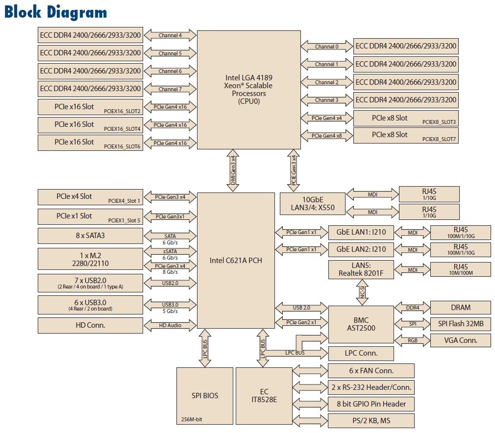
Here's is the first schematic of Intel's upcoming "Whitley" enterprise platform for the upcoming Xeon Scalable "Ice Lake-SP" processors, courtesy momomo_us. The platform sees the introduction of the new LGA4189 socket necessitated by Intel increasing the memory channels per socket to 8, compared to 6 of the current-gen "Cascade Lake-SP." The new platform also sees the introduction of PCI-Express gen 4.0 bus, with each socket putting out up to 64 PCI-Express gen 4.0 CPU-attached lanes. This are typically wired out as three x16 slots, two x8 slots, an x4 chipset bus, and a CPU-attached 10 GbE controller.

The processor supports up to 8 memory channels running at DDR4-3200 with ECC. The other key component of the platform is the Intel C621A PCH. The C621A talks to the "Ice Lake-SP" processor over a PCI-Express 3.0 x4 link, and appears to retain gen 3.0 fabric from the older generation C621. momomo_us also revealed that the 10 nm "Ice Lake-SP" processor could have TDP of up to 270 W.
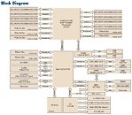
Source: momomo_us (Twitter)
Add your own comment

7 Comments on Intel Whitley Platform for Xeon "Ice Lake-SP" Processors Pictured

#1
AnarchoPrimitiv
Wait, am I reading this correctly? Intel is still using only a 3.0x4 Chipset link for the Xeon platform? I guess they increased the number of CPU lanes (still half that of Epyc), but I was also under the impression that Intel wouldn't have PCIe Gen4 and were going right to PCIe 5.0 with the platform after this one, but I guess I'm misremembering. That's actually one of the best features of TRX40/Eypc in is the 4.0x8 Chipset link, in my opinion, as it essentially removes all potential bottlenecks for even serious storage setups that may have to go through the chipset or allows you to throw a dual port 10GBase-T NIC in there if you had to.

Posted on Reply
#2
efikkan
Well, this seams more like a diagram for a specific motherboard series than the platform.
AnarchoPrimitivWait, am I reading this correctly? Intel is still using only a 3.0x4 Chipset link for the Xeon platform?
<snip>
That's actually one of the best features of TRX40/Eypc in is the 4.0x8 Chipset link, in my opinion, as it essentially removes all potential bottlenecks for even serious storage setups that may have to go through the chipset or allows you to throw a dual port 10GBase-T NIC in there if you had to.
C621A seems like a revision of C621 (the Skylake-SP chipset). So if the chipset doesn't need more, why would you waste more energy and development resources on more?
For servers and high-end workstations, the chipset is pretty much there for convenience. Anything demanding like GPUs, RAID controllers, Optane, PCIe/M2 SSDs, etc. will be connected directly through PCIe.
For example, just look at the schematics in the article, the two 10G NICs are connected directly through PCIe, which is typical for server boards, because if you needed 10G networking, why would you bottleneck the chipset by running it though there? The same is true for large RAIDs, you would hook up a RAID controller, not run it through the chipset. Having most stuff hooked up through the chipset is more a consumer thing.

I'm all for having more stable and mature chipsets. If anything I want less complexity in there and just more CPU PCIe lanes instead.
AnarchoPrimitivI guess they increased the number of CPU lanes (still half that of Epyc), but I was also under the impression that Intel wouldn't have PCIe Gen4 and were going right to PCIe 5.0 with the platform after this one, but I guess I'm misremembering.
More lanes is good, but at least Intel's lanes are working. There is little comfort in having 128 lanes if there are compatibility and stability issues. Let's hope Zen 3 proves to be mature enough to truly compete with Intel.
Posted on Reply
#3
yeeeeman
efikkanWell, this seams more like a diagram for a specific motherboard series than the platform.


C621A seems like a revision of C621 (the Skylake-SP chipset). So if the chipset doesn't need more, why would you waste more energy and development resources on more?
For servers and high-end workstations, the chipset is pretty much there for convenience. Anything demanding like GPUs, RAID controllers, Optane, PCIe/M2 SSDs, etc. will be connected directly through PCIe.
For example, just look at the schematics in the article, the two 10G NICs are connected directly through PCIe, which is typical for server boards, because if you needed 10G networking, why would you bottleneck the chipset by running it though there? The same is true for large RAIDs, you would hook up a RAID controller, not run it through the chipset. Having most stuff hooked up through the chipset is more a consumer thing.

I'm all for having more stable and mature chipsets. If anything I want less complexity in there and just more CPU PCIe lanes instead.


More lanes is good, but at least Intel's lanes are working. There is little comfort in having 128 lanes if there are compatibility and stability issues. Let's hope Zen 3 proves to be mature enough to truly compete with Intel.
Can you give a link where it explains the issues with 128 lanes on zen 2? Thanks
Posted on Reply
#4
Rage Set
efikkanWell, this seams more like a diagram for a specific motherboard series than the platform.


C621A seems like a revision of C621 (the Skylake-SP chipset). So if the chipset doesn't need more, why would you waste more energy and development resources on more?
For servers and high-end workstations, the chipset is pretty much there for convenience. Anything demanding like GPUs, RAID controllers, Optane, PCIe/M2 SSDs, etc. will be connected directly through PCIe.
For example, just look at the schematics in the article, the two 10G NICs are connected directly through PCIe, which is typical for server boards, because if you needed 10G networking, why would you bottleneck the chipset by running it though there? The same is true for large RAIDs, you would hook up a RAID controller, not run it through the chipset. Having most stuff hooked up through the chipset is more a consumer thing.

I'm all for having more stable and mature chipsets. If anything I want less complexity in there and just more CPU PCIe lanes instead.


More lanes is good, but at least Intel's lanes are working. There is little comfort in having 128 lanes if there are compatibility and stability issues. Let's hope Zen 3 proves to be mature enough to truly compete with Intel.
I deploy Epyc and Intel based servers for small to enterprise size businesses and if you're referring to the Epyc NVMe test LTT explored, that is an unreasonable and unrealistic experiment. No one that is an actual IT pro directly attaches that much storage in Raid 0, no less, and expects no issues in performance or most importantly, reliability.

Epyc is hurting Intel right now, unfortunately. There is no need to wait for Zen 3. Intel will come back swinging though, as Enterprise is where the real profit lies.
Posted on Reply
#5
DeathtoGnomes
This sounds like another intel smokescreen, look at my left hand, not the right. This look like a colossal failure and waste of development but intel had to put something out to please the shareholders. yea. :shadedshu:
Posted on Reply
#6
Bones
yeeeemanCan you give a link where it explains the issues with 128 lanes on zen 2? Thanks
+1 to this.
Posted on Reply
#7
DeathtoGnomes
efikkanMore lanes is good, but at least Intel's lanes are working. There is little comfort in having 128 lanes if there are compatibility and stability issues. Let's hope Zen 3 proves to be mature enough to truly compete with Intel.
ya know... I like your enthusiam to discredit AMD any chance you get. Would you go as far as saying intel doesnt share lanes? I can imagine why AMD shares lanes, I'm guessin cuz unused lanes can benefit elsewhere? hmmm
Posted on Reply
Apr 24th, 2024 09:16 EDT change timezone

New Forum Posts

Popular Reviews

Controversial News Posts