Monday, April 19th 2021
GPU Memory Latency Tested on AMD's RDNA 2 and NVIDIA's Ampere Architecture
Graphics cards have been developed over the years so that they feature multi-level cache hierarchies. These levels of cache have been engineered to fill in the gap between memory and compute, a growing problem that cripples the performance of GPUs in many applications. Different GPU vendors, like AMD and NVIDIA, have different sizes of register files, L1, and L2 caches, depending on the architecture. For example, the amount of L2 cache on NVIDIA's A100 GPU is 40 MB, which is seven times larger compared to the previous generation V100. That just shows how much new applications require bigger cache sizes, which is ever-increasing to satisfy the needs.
Today, we have an interesting report coming from Chips and Cheese. The website has decided to measure GPU memory latency of the latest generation of cards - AMD's RDNA 2 and NVIDIA's Ampere. By using simple pointer chasing tests in OpenCL, we get interesting results. RDNA 2 cache is fast and massive. Compared to Ampere, cache latency is much lower, while the VRAM latency is about the same. NVIDIA uses a two-level cache system consisting out of L1 and L2, which seems to be a rather slow solution. Data coming from Ampere's SM, which holds L1 cache, to the outside L2 is taking over 100 ns of latency.
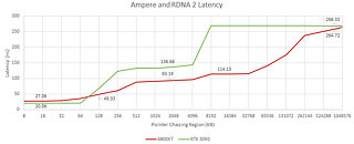 AMD on the other hand has a three-level cache system. There are L0, L1, and L2 cache levels to complement the RDNA 2 design. The latency between the L0 and L2, even with L1 between them, is just 66 ns. Infinity Cache, which is an L3 cache essentially, is adding only additional 20 ns of additional latency, making it still faster compared to NVIDIA's cache solutions. NVIDIA's GA102 massive die seems to represent a big problem for the L2 cache to go around it and many cycles are taken. You can read more about the test here.
Source:
Chips and Cheese
Today, we have an interesting report coming from Chips and Cheese. The website has decided to measure GPU memory latency of the latest generation of cards - AMD's RDNA 2 and NVIDIA's Ampere. By using simple pointer chasing tests in OpenCL, we get interesting results. RDNA 2 cache is fast and massive. Compared to Ampere, cache latency is much lower, while the VRAM latency is about the same. NVIDIA uses a two-level cache system consisting out of L1 and L2, which seems to be a rather slow solution. Data coming from Ampere's SM, which holds L1 cache, to the outside L2 is taking over 100 ns of latency.

92 Comments on GPU Memory Latency Tested on AMD's RDNA 2 and NVIDIA's Ampere Architecture
I agree that 128mb is plenty; I was talking about your comment on the other person, I believe he was referring to the space the cache takes; not the amount of cache.
With 64 MB, it would probably be fine in 1080p, but the hit rate will be much lower in 4K and the card would probably be memory starved. This graph show also why the cards perform so well in 1440p but start to fall behind in 4K. Probably 256 MB would be the perfect spot for 4K.
The thing is Cache are much easier to manufacture (less defect per area) than compute unit. They also consume way less. Also the shorter the data has to travel, the less power it take. The operation itself take very few power but it's moving all the data around that use power. Having a cache that limit the distance data have to travel greatly reduce power consumption.
Also, infinity cache is there to prepare for the next step, Multi chip GPU. but that is another story.
www.techpowerup.com/review/amd-radeon-rx-6900-xt/39.html
See the effects of the Infinity Cache in the charts, 3090 & 6900 trade for FPS, but the 6900 has consistently higher frame rates and fewer low FPS frames, which equates to less laggy feeling, IE... smoothness
It's a marketing point for now, that will lay the work for MCM GPUs next gen. Presumably it makes things smoother for raytracing two as the calculations now involve lookups for more data than that just relevant to the pixels any particular CU is working on, ergo more data being required - but for traditional raster based stuff the HWU video above proves how little it's of benefit to this generation.
That is still significant since a smaller memory bus mean less space used by the memory controller, less pin on the chip, less trace on the cards, simpler card layout, etc...
NVIDIAs "INT units" were stripped down CUDA cores, with Ampere they just cut a little less features (like FP32 capability was stripped out before, but not on Ampere) out from them and started calling them CUDA cores again.
AMD runs everything on same units, just like NVIDIAs full CUDA cores do.
Also, i dont know where you get the idea that cache is the lazy man way of solving things, but it is not. Its actually one of the more critical parts of a chips performance.
RDNA2 doesn't offer any IPC increases over RDNA in the Compute Unit department (new units like Ray Accelerators aside) except for what Infinity Cache brings to the table.
They said it outright on release that RDNA2 offers more performance thanks to three things: Higher clocks, Lower power (per clock) and Infinity Cache bandwidth.
Think about it like case fan hysteresis. If you have a fan curve set up so that they run really quiet and then ramp up significantly once a certain temperature is hit, that's a noticeable change in noise. The change in fan speed is noticeable. However, if you just set a curve that's maybe a little louder initially but a much smoother curve, there's a slow change in RPM, and therefore a less drastic change in noise, which makes it less noticeable to the ear. The same principle applies to frametimes and FPS.
This can add latency. The fact that even with more layer of cache, AMD is able to get lower latency show how well they master the cache thing. They purposely made a lot of effort there because this is a key thing with multi chips modules.
I'm drawing conclusions based on claims by Linus and Anthony, whom both say in the video "I feel like, if my memory serve, etc." hence (my) term "placebo effect" originated.
I'm not going to delve far away from topic, and if you want to establish dominance over my username, by all means you are welcome.
3. It starts to fall behind? N21 has higher performance than Navi10 the higher the resolution is.
If you meant against Ampere, then isn't It actually because Ampere has a lot more Cuda and has a problem with utilization at lower resolutions?
4. Infinity cache has Its advantages, but It also uses up a lot of space. I think It would have been better If N22 had shaved off 32MB, kept only 64MB of IC and added 8 CU instead. N22 is quite Inefficient for an RDNA2 GPU, because It has too high clocks and adding more CU would mean you can clock It lower.
Here is a nice graph of N22 GPU power consumption at different clockspeeds made by uzzi38. Link and another Link
Increasing the clocks from 2295MHz to 2565Mhz caused the power consumption to increase by 59W!
Also, who specifically "mispresented" what, based on your limited understanding?
Also something that i don't have the data on, but since the relation to memory bus/memory size seems clear, it's quite possible that the 96MB block on NAVI 22 have less bandwidth than the 128 MB on Navi 21.
Also, all chip maker have simulator in house. They probably already tested the scenario you propose versus the scenario they choose in simulation and decided that it was not worth it. NAvi 22 aim for 1440P and not 1080P too
I appreciate the effort to look unbiased, but the facts are teh 6900XY is on par with the3090, both of which are unavailable for the masses, and the worst part is that the few who have/can get them will probably use them to mine crypto instead of game on, or test hypothesis like ours, or yours.
Also, if a texture cache is read only how is data ever written to it beyond a driver call for texture, which I am assuming the programmer knew about since they know how to test the cache hierarchy latency on modern GPU's.
Plus Samsungs node and lower clock rate for higher TDP may mean Nvidia had to sacifice latency for stability in higher clock speed with capacitive rolloff effects.
And at the end of the day, AMD is making a product that succeeds despite being 1nm less in process size ( if that actually means anything in the real world) that has significanltly better performance in the 99th percentile meaning less stuttering and better feeling overall performance.
AMD can go up and down, Nvidia still keeps their own. Adding +1 to AMD is not subtracting from the other, per se.
Truth be told, I would like to chime in to the developer side of the equation, but we aren't the who's who of CUDA development the two of us.
PS: I won't sacrifice my integrity for clout.
There is no fundamental relation between global memory (VRMA) and infinity cache either, it's up to AMD to decide how much memory they want, it's just a victim cache.