Monday, November 20th 2023

Intel Lunar Lake-MX SoC with On-Package LPDDR5X Memory Detailed
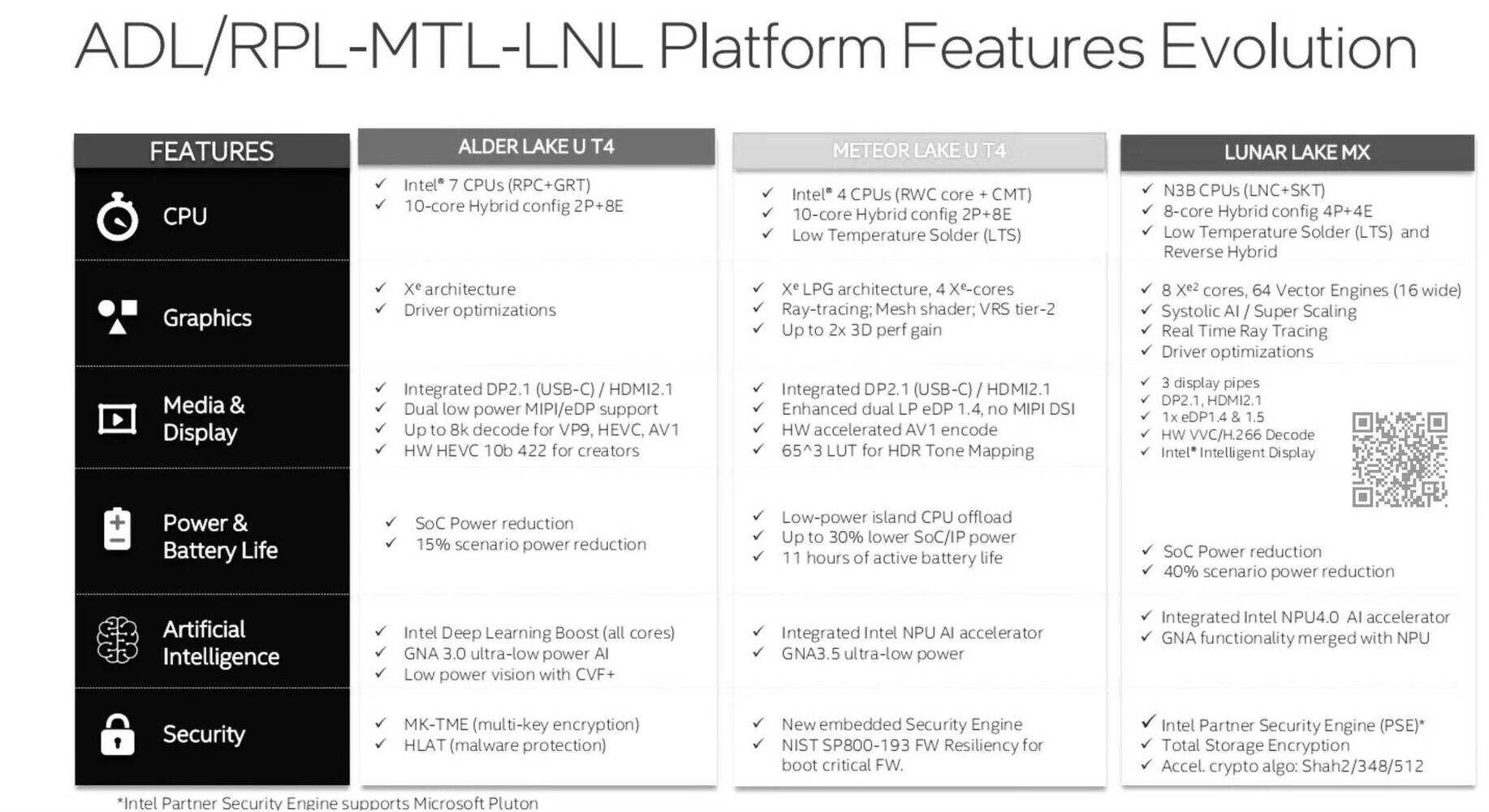
With the reality of high performance Arm processors from Apple and Qualcomm threatening Intel's market share in the client computing space, Intel is working on learner more PCB-efficient client SoCs that can take the fight to them, while holding onto the foundations of x86. The first such form-factor of processors are dubbed -MX. These are essentially -U segment processors with memory on package, to minimize PCB footprint. Intel has fully integrated the PCH into the processor chip with "Meteor Lake," with PCH functions scattered across the SoC and I/O tiles of the processor. An SoC package with dimensions similar to those of -UP4 packages meant for ultrabooks, can now cram main memory, so the PCBs of next-generation notebooks can be further compacted.
Intel had recently shown Meteor Lake-MX packages to the press as a packaging technology demonstration in its Arizona facility. It's unclear whether this could release as actual products, but in a leaked company presentation, confirmed that its first commercial outing will be with Lunar Lake-MX. The current "Alder Lake-UP4" package measures 19 mm x 28.5 mm, and is a classic multi-chip module that combines a monolithic "Alder Lake" SoC die with a PCH die. The "Meteor Lake-UP4" package measures 19 mm x 23 mm, and is a chiplet-based processor, with a Foveros base tile that holds the Compute (CPU cores), Graphics (iGPU), SoC and I/O (platform core-logic) tiles. The "Lunar Lake-MX" package is slightly larger than its -UP4 predecessors, measuring 27 mm x 27.5 mm, but completely frees up space on the PCB for memory.


 The "Lunar Lake-MX" package features a Foveros base tile, just like "Meteor Lake-UP4," but with two LPDDR5X memory chips on package. Depending on the processor model, the memory sizes on offer will be either 16 GB or 32 GB, across a 160-bit dual-channel (4x sub-channel) interface. Memory speeds on offer will be as high as LP5X-8533. Intel is innovating what it calls a "memory side cache," which is an 8 MB fast SRAM cache located somewhere along the memory I/O.
The "Lunar Lake" microarchitecture is expected to see Intel reorganize the various components of the SoC across the tiles. There is expected to be one large logic-heavy tile called the "CPU tile," and a smaller platform core-logic heavy tile called the "SoC tile." With Lunar Lake, Intel Foundry Services (IFS) is expected to debut the company Intel 18A foundry node, which offers transistor densities and power/thermal characteristics comparable to 2 nm-class nodes by TSMC. From the looks of it, the entire CPU tile will be built on the TSMC N3B (3 nm) foundry node.


 The CPU tile contains the compute complex along the high bandwidth North Fabric. The key components here are the Performance Compute cores, the Low-Power core clusters; the next-generation NPU which accelerates AI, the iGPU based on the Xe2 "Battlemage" graphics architecture, and the LPDDR5X memory controllers. There are other minor bandwidth-hungry components, such as the IPU (image processing), and media engine (video accelerators). The SoC die is now back to being a glorified PCH, with the various platform interfaces, PCIe, USB, and Thunderbolt I/O.
The compute muscle of "Lunar Lake-MX" will see a CPU with a 4P+4E configuration, with a very high degree of interoperability integration with the OS. The performance cores (P-cores) are codenamed "Lion Cove," and will be three generations ahead of the current "Raptor Cove," which means three consecutive cycles of IPC uplifts. The efficiency cores (E-cores) are codenamed "Skymont" and will be two generations ahead of the current "Gracemont." The upcoming "Crestmont" E-core architecture will be deployed on "Meteor Lake" and "Arrow Lake."
The graphics muscle is care of the Xe²-LPG graphics architecture, which draws from Intel's next-generation gaming graphics architecture codenamed "Battlemage." The iGPU on the "Lunar Lake-MX" package has 8 Xe cores worth 64 16-wide vector engines, full DirectX 12 Ultimate API feature-set, and hardware support for Intel's next systolic AI superscaling technology.
We are still far away from actual processor model numbers and SKUs, but Intel has drawn up some draft SKU segmentation for "Lunar Lake-MX." It sees 32 GB and 16 GB variants of Core 7 SKUs with 4P+4E CPUs and 8 Xe cores; and 32 GB and 16 GB variants of Core 5 SKUs with 4P+4E CPUs, and 7 Xe cores. Intel is targeting power envelopes as low as 8 W, for completely fanless devices, going all the way up to 30 W for high performance variants. The company aims for "Lunar Lake-MX" to compete in the same device category as the 2025 successors of Apple M3.
Sources:
VideoCardz, Geddagod (AnandTech forums), Andreas Schilling (Twitter), Yuuki_Ans (Twitter)
Intel had recently shown Meteor Lake-MX packages to the press as a packaging technology demonstration in its Arizona facility. It's unclear whether this could release as actual products, but in a leaked company presentation, confirmed that its first commercial outing will be with Lunar Lake-MX. The current "Alder Lake-UP4" package measures 19 mm x 28.5 mm, and is a classic multi-chip module that combines a monolithic "Alder Lake" SoC die with a PCH die. The "Meteor Lake-UP4" package measures 19 mm x 23 mm, and is a chiplet-based processor, with a Foveros base tile that holds the Compute (CPU cores), Graphics (iGPU), SoC and I/O (platform core-logic) tiles. The "Lunar Lake-MX" package is slightly larger than its -UP4 predecessors, measuring 27 mm x 27.5 mm, but completely frees up space on the PCB for memory.


The "Lunar Lake" microarchitecture is expected to see Intel reorganize the various components of the SoC across the tiles. There is expected to be one large logic-heavy tile called the "CPU tile," and a smaller platform core-logic heavy tile called the "SoC tile." With Lunar Lake, Intel Foundry Services (IFS) is expected to debut the company Intel 18A foundry node, which offers transistor densities and power/thermal characteristics comparable to 2 nm-class nodes by TSMC. From the looks of it, the entire CPU tile will be built on the TSMC N3B (3 nm) foundry node.


The compute muscle of "Lunar Lake-MX" will see a CPU with a 4P+4E configuration, with a very high degree of interoperability integration with the OS. The performance cores (P-cores) are codenamed "Lion Cove," and will be three generations ahead of the current "Raptor Cove," which means three consecutive cycles of IPC uplifts. The efficiency cores (E-cores) are codenamed "Skymont" and will be two generations ahead of the current "Gracemont." The upcoming "Crestmont" E-core architecture will be deployed on "Meteor Lake" and "Arrow Lake."
The graphics muscle is care of the Xe²-LPG graphics architecture, which draws from Intel's next-generation gaming graphics architecture codenamed "Battlemage." The iGPU on the "Lunar Lake-MX" package has 8 Xe cores worth 64 16-wide vector engines, full DirectX 12 Ultimate API feature-set, and hardware support for Intel's next systolic AI superscaling technology.
We are still far away from actual processor model numbers and SKUs, but Intel has drawn up some draft SKU segmentation for "Lunar Lake-MX." It sees 32 GB and 16 GB variants of Core 7 SKUs with 4P+4E CPUs and 8 Xe cores; and 32 GB and 16 GB variants of Core 5 SKUs with 4P+4E CPUs, and 7 Xe cores. Intel is targeting power envelopes as low as 8 W, for completely fanless devices, going all the way up to 30 W for high performance variants. The company aims for "Lunar Lake-MX" to compete in the same device category as the 2025 successors of Apple M3.
30 Comments on Intel Lunar Lake-MX SoC with On-Package LPDDR5X Memory Detailed
The first on-package Atom was even before that with the Smartphone oriented Medfield in 2012: www.anandtech.com/show/5365/intels-medfield-atom-z2460-arrive-for-smartphones/1
Meteorlake will also have some on-package DRAM variants, but unlike Lunar Lake it doesn't claim to be a big advance in mobility, so it'll be only available in certain variants while for Lunar Lake it'll have it for all.
www.tomshardware.com/news/intel-demos-meteor-lake-cpu-with-on-package-lpddr5xLPCAMM is nowhere near low power or compact enough for what's going in Lunar Lake. It will be more than before sure.Intel 4 doesn't have enough libraries for Lunar Lake, period. Not fully sure about Intel 3, but they admit that they won't really get ahead until 18A, and Intel 3 is going to be using a ton of wafers because both E and P core Xeons are going to be using them and they are all very large dies. Granite Rapids-SP has two compute tiles with over 500mm2 size, while -AP version has three. Sierra Forest-SP has 1x 500mm2+ die, while -AP has 2x.
20A is same as Intel 4 in that it doesn't have enough libraries. If Intel keeps using TSMC for main chip compute tile by 18A, then it's a problem, but until then, there are legitimate reasons for doing what they are doing. When it comes to Intel 3 and 18A being foundry-oriented process, the reason is same. Only those two have all the libraries required, while 4 and 20A contains enough blocks for CPU to rapidly iterate to next generation. With Lunar Lake coming sometime next year and 18A not being production-ready until end of next year, 18A is a no-go.
Lunar Lake was conceived around the time when Apple abandoned Intel, and future of their manufacturing was murky. But as of right now multiple reports state manufacturing is now going full steam while design team is still meh. The design team had been hiding behind massive process lead, and this loss exposes them.
Gelsinger is bringing changes and new metrics to bring accountability for the design team, so hopefully they'll do better. The design team was doing appalling things such as directing the process team to change the metrics to fit their needs, rather than working with what they have. Now, the goal is the design team is essentially treated little more than 3rd party.Leaked slides show that I/O die for Granite Rapids and Sierra Forest use Intel 7, while compute tile uses Intel 3. As I said the compute tiles for both are over 500mm2. Rough analysis got 510mm2. So it's in the ballpark of 500mm2. Yea they have three compute size variants but regardless these tiles are massive.
The Intel 3 and 18A is more than a plus. It's more like 10nm SF and Intel 7, but without the density loss SF and 7 brought. The numerous plusses in 14nm only brought about 4-5% gains, while 3 gains 18% alone, and will have density advantage for high performance libraries(so for successors to Meteorlake), while 3 has full set of libraries for I/O, GPU, CPU, and so on, while 4 is bare minimum.
You do know Knights Landing has come out and shipped to many units right? You could even get a socketed variant in a ATX tower format and boot itself and run Cinebench on it.
Everyone:
On-package memory for Meteor and Lunar is for space savings for 99% of the scenarios. I doubt it even saves noticeable amount of standby power. Yes, you need on-package/soldered for such fast memory, but the power savings come from being the LPDDR standard.
There are basically three "on-package memory" variants.
1. eDRAM as with Broadwell, with proprietary connections and very low latency and high bandwidth
2. HBM, which is for bandwidth and space savings
3. On package system memory. Mostly for space savings.
The three are very, very different.
These slides also show the CPU and a relatively large Battlemage GPU sharing the same tile. That rules out IFS 20A because it won't have the high density libraries needed to make a GPU and IFS 3 won't be efficient enough and IFS 18A won't be ready in time. TSMC N4 also won't be good enough. So the only possible option is one of the TSMC N3 nodes, which fits because the Battlemage GPU is also likely to be made on that node. Now that SoC tile could be a little more flexible.
This also explains why TSMC is making the CPU tile. Even if Intel delivers all of their new nodes on the schedule they claim, none of them can build this particular CPU tile by the end of 2024.
Now I think I can infer a little more. (Everything I say after this point is speculation.) Aside from the cost of designing new microarchitectures and new manufacturing nodes, there's also a bit of cost designing and making each final package. The Lunar Lake tiles are completely incompatible with the Meteor Lake package, but the Arrow Lake image here looks just like Meteor Lake's package. So I think Lunar Lake will cover all of the 8-15W market (4P+4E, some with on-package memory and some with off-package memory), and Arrow Lake will take the 28W market (2LPE+6P+8E) and up (2LPE+8P+16E). Lunar Lake alone will have Battlemage graphics, as Arrow Lake will reuse the Meteor Lake GPU tiles. Arrow Lake in the 28W market will reuse every tile from Meteor Lake except the CPU tile, which means it'll have 2 low power Crestmont cores, 6 Lion Cove performance cores, and 8 Skymont "efficiency" cores. Arrow Lake for desktops will inherit the 8P+16E configuration from Raptor Lake, probably with a new SoC, either built with TSMC N6 without the low power cores or IFS 3 with 2 Skymont cores.
Panther Lake is next in the lineup, probably for 2025 when IFS 18A is ready.
The article mentions that Lunar Lake MX has a 160-bit memory interface, which would be very helpful for the GPU, but the slides only say dual channel which normally is 128 bit. Software stores things in memory in 64-bit chunks, so 160-bits would be a little unconventional for CPU memory.
Another interesting detail in the slides is that the Core 7 is "8 Core 12M". A similar Meteor Lake configuration would be 8 cores and 12 threads. So what's "12M"? Does this relate to the rumor that Intel is replacing Hyperthreading?
I think the excess bits are for ECC even though, going by this article from Synopsys, ECC in LPDDR is usually not implemented by adding bits to the memory bus ("side-band ECC") but rather in other ways.