Monday, July 20th 2026

Per-Module GDDR7 Temperature Reading Unlocked on NVIDIA GeForce RTX 50 "Blackwell"

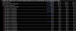
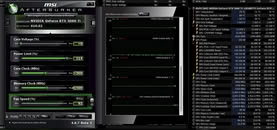
More individual readings are being unlocked on NVIDIA's GeForce RTX 50 series "Blackwell" graphics cards, as the modding community has started exploring GDDR7 temperature monitoring on a per-module basis. Interestingly, the modding community is diverse this time, including contributions from Brazilian GPU repair specialist Paulo Gomes, MSI Afterburner developer "Unwinder," Overclock.net member "asder00," HWiNFO creator Martin "Mumak" Malík, and Linux code developer "olealgoritme." By joining forces, the team managed to create a plugin for MSI Afterburner that provides access to individual, per-module GDDR7 temperature readings.

This new Hotspot.dll plugin, which previously only provided access to the hidden "Blackwell" GPU die, is now updated to handle GDDR7 temperature readings, unlocking the GDDR7 thermal sensors hidden inside memory ICs. For example, on the GeForce RTX 5090 GPU, there are 16 GDDR7 memory modules, each with a 2 GB capacity. Since there are 16 chips, the tool can read 16 temperature sensors and provide 16 individual readings. However, some GDDR7-equipped "Blackwell" GPUs use a clamshell memory configuration, meaning the GDDR memory is on both sides of the PCB. For example, in the case of the RTX PRO 6000 "Blackwell", this would mean only half the measurement points, as the GDDR7 memory is present in 16 locations on both sides of the PCB, for a total of 32 memory modules.
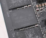
Nonetheless, the addition of individual memory IC temperature readings is very helpful, especially when troubleshooting the GPU. When a GDDR7 memory module is not properly cooled, particularly if the thermal pad that should be present wears out or is missing, the module can overheat and reach the end of its life. Therefore, proper detection is always a good idea. With hotspot readings on the GPU die, hotspot delta, memory junction, and GDDR7 memory readings, NVIDIA's "Blackwell" is finally fully unlocked in terms of measurement.
Source: via VideoCardz
Add your own comment

36 Comments on Per-Module GDDR7 Temperature Reading Unlocked on NVIDIA GeForce RTX 50 "Blackwell"

#1
Kwadratowicz
Trrrryt
AleksandarKHowever, some GDDR7-equipped "Blackwell" GPUs use a clamshell memory configuration, meaning the GDDR memory is on both sides of the PCB. For example, in the case of the RTX 5090, this would mean only half the measurement points, as the GDDR7 memory is present in eight locations on both sides of the PCB.
I don't agree with that statement, cause even now with different made gpus the backplate can get toasty, where the front of the card is cooled properly, sometimes back is not cooled at all, so I'm curious if there will be significant difference in temperature on those cards :D
Posted on Reply
#2
soder
KwadratowiczI don't agree with that statement, cause even now with different made gpus the backplate can get toasty, where the front of the card is cooled properly, sometimes back is not cooled at all, so I'm curious if there will be significant difference in temperature on those cards :D
Do you own a 5090? If not, why do you even worry about such thing?
Posted on Reply
#3
Kwadratowicz
Trrrryt
soderDo you own a 5090? If not, why do you even worry about such thing?
Cause I like data and stats :D tables in excel, temperatures of other things the sheer idea that people found how to use something manufacturer has hidden :D
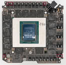
Posted on Reply
#4
_JP_
Reminds me of the sensor density that 2008~2016 high-end cards had, exactly to boost their potential to be OC'd and break records. :oops:
Right now, it's great to have them so that we have some sort of EAS that the card is about to burn itself. :laugh:
Posted on Reply
#5
SnoutBaron
AleksandarKMore individual readings are being unlocked on NVIDIA's GeForce RTX 50 series "Blackwell" graphics cards, as the modding community has started exploring GDDR7 temperature monitoring on a per-module basis. Interestingly, the modding community is diverse this time, including contributions from Brazilian GPU repair specialist Paulo Gomes, MSI Afterburner developer "Unwinder," Overclock.net member "asder00," HWiNFO creator Martin "Mumak" Malík, and Linux code developer "olealgoritme." By joining forces, the team managed to create a plugin for MSI Afterburner that provides access to individual, per-module GDDR7 temperature readings.

This new Hotspot.dll plugin, which previously only provided access to the hidden "Blackwell" GPU die, is now updated to handle GDDR7 temperature readings, unlocking the GDDR7 thermal sensors hidden inside memory ICs. For example, on the GeForce RTX 5090 GPU, there are 16 GDDR7 memory modules, each with a 2 GB capacity. Since there are 16 chips, the tool can read 16 temperature sensors and provide 16 individual readings. However, some GDDR7-equipped "Blackwell" GPUs use a clamshell memory configuration, meaning the GDDR memory is on both sides of the PCB. For example, in the case of the RTX 5090, this would mean only half the measurement points, as the GDDR7 memory is present in eight locations on both sides of the PCB.

Nonetheless, the addition of individual memory IC temperature readings is very helpful, especially when troubleshooting the GPU. When a GDDR7 memory module is not properly cooled, particularly if the thermal pad that should be present wears out or is missing, the module can overheat and reach the end of its life. Therefore, proper detection is always a good idea. With hotspot readings on the GPU die, hotspot delta, memory junction, and GDDR7 memory readings, NVIDIA's "Blackwell" is finally fully unlocked in terms of measurement.
I don't want to speak for Unwinder, but over on Guru3D, he did make it clear that he is not allowed to release non-official sensors like this for Afterburner but that RTSS is another story, and that officially it is not him but rather him saying...if they were to do it....how to do it wink wink.


Posted on Reply
#6
lepudruk
There is already a topic on the forum regarding this. From what people are publishing, the range of results is quite large. This may be due to differences in the construction of individual models, manufacturer designs, or even the time that has passed since the thermal paste was applied.

Post your RTX 5xxx series hotspot temp.
Posted on Reply
#7
wNotyarD
lepudrukThere is already a topic on the forum regarding this. From what people are publishing, the range of results is quite large. This may be due to differences in the construction of individual models, manufacturer designs, or even the time that has passed since the thermal paste was applied.

Post your RTX 5xxx series hotspot temp.
That was only for the core hotspot. Now per memory module temperature reading has been unlocked.
Posted on Reply
#8
Grimling
Good to see that people who own a 50 series GPU have now full access to the temperature telemetry of those cards!
The question is, why does Nvidia do censor those monitoring APIs?
Just because they are evil?
Or to "protect" the user?
NVIDIA certainly has not publicly explained why some temperature telemetry on many GeForce RTX 50-series cards was initially unavailable through the usual monitoring APIs.
Posted on Reply
#9
Gucky
Its just another way to help diagnosing. This can show irregularities like a thermalpads that are bad or have bad contact.
AleksandarKFor example, in the case of the RTX 5090, this would mean only half the measurement points, as the GDDR7 memory is present in eight locations on both sides of the PCB.
Huh? Since when does the 5090 have clamshell VRAM? Its all 16 chips on one side. You mean a RTX 6000 Pro Blackwell.
soderDo you own a 5090? If not, why do you even worry about such thing?
I owned a 3090 and it was the case of very hot backside VRAM.

My current 5090 has VRAM temps below 80°C at ~600W and below 70°C at ~400W.
Even the GPU-Hotspot is below 70°C at 400W. And I am at ~350W for my 24/7 gaming settings.
Posted on Reply
#10
A Computer Guy
This might make for some interesting comparisons for those with Gigabyte cards using Gigaslop putty vs. putty replaced with thermal pads.
Posted on Reply
#11
wolf
Better Than Native
GrimlingThe question is, why does Nvidia do censor
Suggesting it's evil is certainly a take.

I tend to think that it just barely matters to the vast majority of users, and numbers can confuse them and cause them to think something is wrong when it isn't.

Easier to obfuscate it for everyone and perplex very few as to why, than worry perhaps far more over absolutely nothing.
Posted on Reply
#12
Grimling
wolfI tend to think that it just barely matters to the vast majority of users, and numbers can confuse them and cause them to think something is wrong when it isn't.
But if that is the case, why was that never a problem before? Are people just suddenly confused about Hotspot temps out of nothing? And the people that could be confused about the hotspot temps, are those the kind of people running HWinfo and furmark to stress out the card and specifically look for the hotspot temp? I do not think so. Probably that are rather people who would not even be aware of what a furmark is.
Posted on Reply
#13
Kwadratowicz
Trrrryt
wolfI tend to think that it just barely matters to the vast majority of users, and numbers can confuse them and cause them to think something is wrong when it isn't.
GrimlingBut if that is the case, why was that never a problem before?
If someone is switching from older hardware that is cool and quiet to behemoth of todays era they could really think there is something wrong with hardware.
I was trying to cool My 9070 xt cause GPU that is over 75C was for me unthinkable stuff, I've had 1070 ti which never exceeded 75C (while working normally) and was dead quiet with deshroud mod.
The stuff that is newer is more power hungry and warmer, the cooling capabilities for smaller nodes is problematic too, cause higher density tends to lead to higher temperatures even with proper cooling.
When I've changed from 1070 ti to 9070 xt, and from 2700 ryzen to 5700x I was dumbfounded why it is warmer even 2700 and 5700x are both 65W cpu.
Posted on Reply
#14
wolf
Better Than Native
GrimlingBut if that is the case, why was that never a problem before?
It has caused grief before, both for Nvidia and AMD, neither of which has en masse RMA rates from cooked memory, it was just alarming to see big number.

But hey maybe you're right, it's just Jensen's law of Sensor Deprivation because he's evil.
Posted on Reply
#16
agent_x007
Is there a map of where each chip is on actual PCB ? (ie. sensor with name "xyz" is "a" chips away clockwise from top left PCB corner on PCB [for example])
Can manufacturers mixed where each chip is on PCB ? (sensor name "xyz" is in different place between MSI and Gigabyte PCBs)
Is VRAM chip "GDDR7 0A" (0 - channel, A-subchannel), always in the same spot on ASUS and Gigabyte ?
Posted on Reply
#17
Space Lynx
Astronaut
This is kind of neat, I like to monitor my temps sometimes in more detail, and if I ever do a thermal pad swap on the vram someday, this will come in handy so I can monitor I applied it correctly or not.
Posted on Reply
#18
SnoutBaron
wolfIt has caused grief before, both for Nvidia and AMD, neither of which has en masse RMA rates from cooked memory, it was just alarming to see big number.

But hey maybe you're right, it's just Jensen's law of Sensor Deprivation because he's evil.
I've already seen comments on YouTube wanting to RMA their 50 series card because they saw high 90s hotspot with 20C deltas.

I can understand why Nvidia didn't want these sensors public.
Posted on Reply
#19
Grimling
SnoutBaronI can understand why Nvidia didn't want these sensors public.
then why even allow access to any sensor data? Maybe even the FAN-Speed Data is too much for people these days.
"I expected 1666 RPM of Fan-speed at max, but my card has 2122 RPM under full load! I RMA this Card!"
Posted on Reply
#20
rusTORK
SnoutBaronI can understand why Nvidia didn't want these sensors public.
NVIDIA & vendors saved $0.25 on decent thermal pads for GDDR6X chips on RTX 3000 and that caused it's overheating. Replacement pads on proper one (with higher rating) solved problem with overheating completely.

So, always same story - it's all about money (save them).
Posted on Reply
#21
SnoutBaron
Grimlingthen why even allow access to any sensor data? Maybe even the FAN-Speed Data is too much for people these days.
"I expected 1666 RPM of Fan-speed at max, but my card has 2122 RPM under full load! I RMA this Card!"
Because Nvidia also have large multi-billion dollar OEM partners who need to check for issues, and thus those sensors were, until now, only accessible with special software from Nvidia.
Posted on Reply
#22
wolf
Better Than Native
Grimlingthen why even allow access to any sensor data? Maybe even the FAN-Speed Data is too much for people these days.
"I expected 1666 RPM of Fan-speed at max, but my card has 2122 RPM under full load! I RMA this Card!"
The point is that exposing a number without context creates support noise from people who see "90°C" and assume catastrophe, despite the component being designed for it. Turning that into "why have any sensors at all?" is a textbook strawman.
Posted on Reply
#23
Grimling
wolfThe point is that exposing a number without context creates support noise from people who see "90°C" and assume catastrophe, despite the component being designed for it. Turning that into "why have any sensors at all?" is a textbook strawman.
Again, any number you expose (including FAN-Speed and maybe even FPS) will create "support noise from people". So if the reason for Nvidia, to censor Hotspot and Memory Data, is, to reduce or eliminate "support noise from people", then it would be logical to remove ANY ACCESS to ANY telemetry on ANY Card, and make these APIs only available to Nvidia certified technicians!
Posted on Reply
#24
SnoutBaron
agent_x007Is there a map of where each chip is on actual PCB ? (ie. sensor with name "xyz" is "a" chips away clockwise from top left PCB corner on PCB [for example])
Can manufacturers mixed where each chip is on PCB ? (sensor name "xyz" is in different place between MSI and Gigabyte PCBs)
Is VRAM chip "GDDR7 0A" (0 - channel, A-subchannel), always in the same spot on ASUS and Gigabyte ?
Apparently Nvidia has kept this configuration since Pascal at least Kepler.
Memory modules/chips are counted counter-clockwise, starting from the opposite corner of the golden arrow (or orientation marker) on the GPU core/die.


EDIT: And here's a PNY 5090

Source: Northwest Repair


And Titan Z

Posted on Reply
#25
PixelTech
I'm guessing that if NV was pressed on the reason why, it's that these temp sensors aren't accurate.
Otherwise, hiding sensors or choosing to not let general consumers know the hotspot temps seems easily grouped in without the general practice by companies to not include manual diagrams for repairing. Moves to remove Right to Repair/Anti-Consumer.
We should remember:

NV is an AI company now. We're on the last of their list of caring. Don't expect anything positive from them.
Posted on Reply
Add your own comment
Nov 20th, 2026 19:26 PST change timezone

New Forum Posts

Popular Reviews

TPU on YouTube

Controversial News Posts