News Posts matching #GDDR7

Return to Keyword Browsing

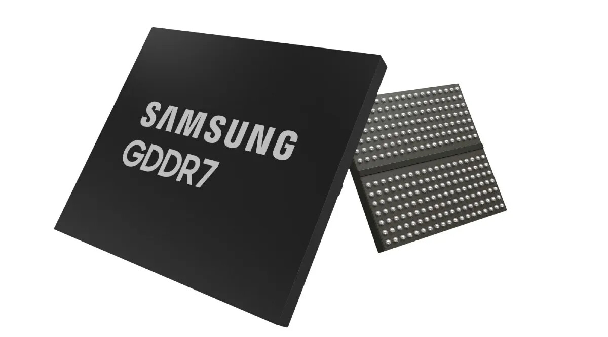
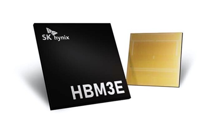
Introspect Technology Ships World's First GDDR7 Memory Test System

Introspect Technology, a JEDEC member and a leading manufacturer of test and measurement instruments, announced today that it has shipped the M5512 GDDR7 Memory Test System, the world's first commercial solution for testing JEDEC's newly minted JESD239 Graphics Double Data Rate (GDDR7) SGRAM specification. This category-creating solution enables graphics memory engineers, GPU design engineers, product engineers in both memory and GPU spaces, and system integrators to rapidly bring up new GDDR7 memory devices, debug protocol errors, characterize signal integrity, and perform detailed memory read/write functional stress testing without requiring any other tool.

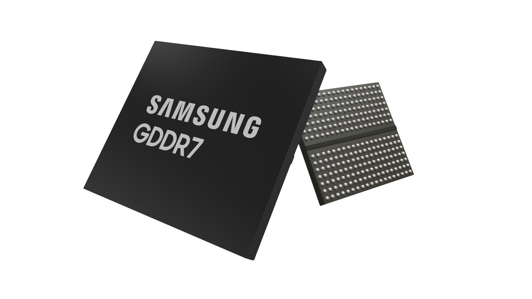
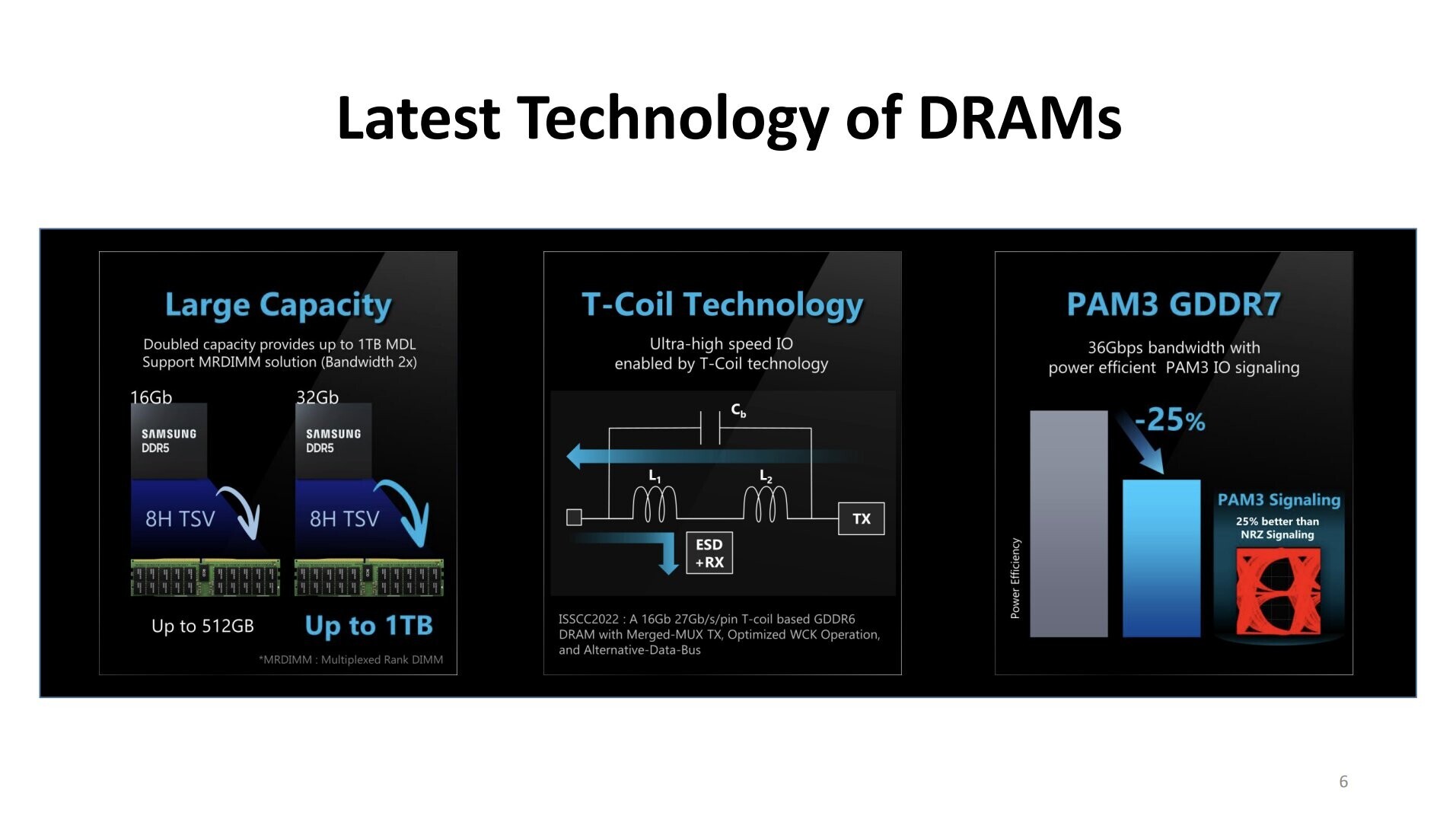
The GDDR7 specification is the latest industry standard that is aimed at the creation of high-bandwidth and high-capacity memory implementations for graphics processing, artificial intelligence (AI), and AI-intensive networking. Featuring pulse-amplitude modulation (PAM) and an improved signal to noise ratio compared to other PAM4 standards used in networking, the GDDR7 PAM3 modulation technology achieves greater power-efficiency while significantly increasing data transmission bandwidth over constrained electrical channels.

Product Pages of Samsung 28 Gbps and 32 Gbps GDDR7 Chips Go Live

Samsung is ready with a GDDR7 memory chip rated at an oddly-specific 28 Gbps. This speed aligns with the reported default memory speeds of next-generation NVIDIA GeForce RTX "Blackwell" GPUs. The Samsung GDDR7 memory chip bearing model number K4VAF325ZC-SC28, pictured below, ticks at 3500 MHz, yielding 28 Gbps (GDDR7-effective) memory speeds, and comes with a density of 16 Gbit (2 GB). This isn't Samsung's only GDDR7 chip at launch, the company also has a 32 Gbps high performance part that it built in hopes that certain high-end SKUs or professional graphics cards may implement it. The 32 Gbps GDDR7 chip, bearing the chip model number K4VAF325ZC-SC32, offers the same 16 Gbit density, but at a higher 4000 MHz clock. The Samsung website part-identification pages for both chips say that the parts are sampling to customers, which is usually just before it enters mass-production, and is marked "shipping."

SK hynix Presents the Future of AI Memory Solutions at NVIDIA GTC 2024

SK hynix is displaying its latest AI memory technologies at NVIDIA's GPU Technology Conference (GTC) 2024 held in San Jose from March 18-21. The annual AI developer conference is proceeding as an in-person event for the first time since the start of the pandemic, welcoming industry officials, tech decision makers, and business leaders. At the event, SK hynix is showcasing new memory solutions for AI and data centers alongside its established products.

Showcasing the Industry's Highest Standard of AI Memory
The AI revolution has continued to pick up pace as AI technologies spread their reach into various industries. In response, SK hynix is developing AI memory solutions capable of handling the vast amounts of data and processing power required by AI. At GTC 2024, the company is displaying some of these products, including its 12-layer HBM3E and Compute Express Link (CXL)1, under the slogan "Memory, The Power of AI". HBM3E, the fifth generation of HBM2, is the highest-specification DRAM for AI applications on the market. It offers the industry's highest capacity of 36 gigabytes (GB), a processing speed of 1.18 terabytes (TB) per second, and exceptional heat dissipation, making it particularly suitable for AI systems. On March 19, SK hynix announced it had become the first in the industry to mass-produce HBM3E.

NVIDIA to Implement GDDR7 Memory on Top-3 "Blackwell" GPUs

NVIDIA is confirmed to implement the GDDR7 memory standard with the top three GPU ASICs powering the next-generation "Blackwell" GeForce RTX 50-series, Tweaktown reports, citing XpeaGPU. By this, we mean the top three physical silicon types from which NVIDIA will carve out the majority of its SKUs. This would include the GB202, the GB203, and GB205; which will power successors to everything from the current RTX 4070 to the RTX 4090. NVIDIA is expected to build these chips on the TSMC 4N foundry node.

There will be certain GPU ASIC types in the "Blackwell" generation that will stick to older memory standards such as GDDR6 or even the GDDR6X. These would be successors to the current AD106 and AD107 ASICs, powering SKUs such as the RTX 4060 Ti, and below. NVIDIA co-developed the GDDR6X standard with Micron Technology, which is the chip's exclusive supplier to NVIDIA. GDDR6X scales up to 23 Gbps and 16 Gbit, which means NVIDIA can avail plenty of performance for the lower-end of its product stack using GDDR6X; especially considering that its GDDR7 implementation will only run at 28 Gbps, despite chips being available in the market for 32 Gbps, or even 36 Gbps. Even if NVIDIA chooses the regular GDDR6 standard for its entry-mainstream chips, the tech scales up to 20 Gbps.

SK hynix Unveils Highest-Performing SSD for AI PCs at NVIDIA GTC 2024

SK hynix unveiled a new consumer product based on its latest solid-state drive (SSD), PCB01, which boasts industry-leading performance levels at GPU Technology Conference (GTC) 2024. Hosted by NVIDIA in San Jose, California from March 18-21, GTC is one of the world's leading conferences for AI developers. Applied to on-device AI PCs, PCB01 is a PCIe fifth-generation SSD which recently had its performance and reliability verified by a major global customer. After completing product development in the first half of 2024, SK hynix plans to launch two versions of PCB01 by the end of the year which target both major technology companies and general consumers.

Optimized for AI PCs, Capable of Loading LLMs Within One Second
Offering the industry's highest sequential read speed of 14 gigabytes per second (GB/s) and a sequential write speed of 12 GB/s, PCB01 doubles the speed specifications of its previous generation. This enables the loading of LLMs required for AI learning and inference in less than one second. To make on-device AIs operational, PC manufacturers create a structure that stores an LLM in the PC's internal storage and quickly transfers the data to DRAMs for AI tasks. In this process, the PCB01 inside the PC efficiently supports the loading of LLMs. SK hynix expects these characteristics of its latest SSD to greatly increase the speed and quality of on-device AIs.

Samsung Shows Off 32 Gbps GDDR7 Memory at GTC

Samsung Electronics showed off its latest graphics memory innovations at GTC, with an exhibit of its new 32 Gbps GDDR7 memory chip. The chip is designed to power the next generation of consumer and professional graphics cards, and some models of NVIDIA's GeForce RTX "Blackwell" generation are expected to implement GDDR7. The chip Samsung showed off at GTC is of the highly relevant 16 Gbit density (2 GB). This is important, as NVIDIA is rumored to keep graphics card memory sizes largely similar to where they currently are, while only focusing on increasing memory speeds.

The Samsung GDDR7 chip shown is capable of its 32 Gbps speed at a DRAM voltage of just 1.1 V, which beats the 1.2 V that's part of JEDEC's GDDR7 specification, which along with other power management innovations specific to Samsung, translates to a 20% improvement in energy efficiency. Although this chip is capable of 32 Gbps, NVIDIA isn't expected to give its first GeForce RTX "Blackwell" graphics cards that speed, and the first SKUs are expected to ship with 28 Gbps GDDR7 memory speeds, which means NVIDIA could run this Samsung chip at a slightly lower voltage, or with better timings. Samsung also made some innovations with the package substrate, which decreases thermal resistance by 70% compared to its GDDR6 chips. Both NVIDIA and AMD are expected to launch their first discrete GPUs implementing GDDR7, in the second half of 2024.

NVIDIA GeForce RTX 50-series "Blackwell" to use 28 Gbps GDDR7 Memory Speed

The first round of NVIDIA GeForce RTX 50-series "Blackwell" graphics cards that implement GDDR7 memory are rumored to come with a memory speed of 28 Gbps, according to kopite7kimi, a reliable source with NVIDIA leaks. This is despite the fact that the first GDDR7 memory chips will be capable of 32 Gbps speeds. NVIDIA will also stick with 16 Gbit densities for the GDDR7 memory chips, which means memory sizes could remain largely unchanged for the next generation; with the 28 Gbps GDDR7 memory chips providing 55% higher bandwidth over 18 Gbps GDDR6 and 33% higher bandwidth than 21 Gbps GDDR6X. It remains to be seen what memory bus widths NVIDIA chooses for its individual SKUs.

NVIDIA's decision to use 28 Gbps as its memory speeds has some precedent in recent history. The company's first GPUs to implement GDDR6, the RTX 20-series "Turing," opted for 14 Gbps speeds despite 16 Gbps GDDR6 chips being available. 28 Gbps is exactly double that speed. Future generations of GeForce RTX GPUs, or even refreshes within the RTX 50-series could see NVIDIA opt for higher memory speeds such as 32 Gbps. When the standard debuts, companies like Samsung even plan to put up fast 36 Gbps chips. Besides a generational doubling in speeds, GDDR7 is more energy-efficient as it operates at lower voltages than GDDR6. It also uses a more advanced PAM3 physical layer signaling compared to NRZ for JEDEC-standard GDDR6.

First GPUs Implementing GDDR7 Memory Could Stick with 16 Gbit Chips, 24 Gbit Possible

Some of the first gaming GPUs that implement the next-generation GDDR7 memory standard, will stick to 16 Gbit memory chip densities (2 GB), according to kopite7kimi, a reliable source with NVIDIA GeForce leaks. 16 Gbit is what is standard for the current RTX 40-series graphics cards, which ensures that a GPU with 256-bit memory bus gets 16 GB of video memory; the ones with 192-bit get 12 GB; and the ones with 128-bit get 8 GB. The flagship RTX 4090 uses twelve of these chips over its 384-bit memory bus for 24 GB.

Kopite7kimi's leak could have a different connotation, that much like the RTX 30-series "Ampere" and RTX 40-series "Ada," NVIDIA might not use JEDEC-standard GDDR7 on all product segments, and might co-engineer an exclusive standard with a DRAM company with memory bus signaling and power management technologies most optimal to its graphics architecture. It co-developed the GDDR6X with Micron Technology to do exactly this. GDDR7 comes with data-rates as high as 32 Gbps, which will be the top speed for the first round of GDDR7 chips that come out toward the end of 2024, heading into 2025. The second round of GDDR7 chips slated for late-2025 going into 2026, could go as fast as 36 Gbps. This is similar to how the first GDDR6 chips were 14-16 Gbps, and the next round did 18-20 Gbps.

JEDEC Publishes GDDR7 Graphics Memory Standard

JEDEC Solid State Technology Association, the global leader in the development of standards for the microelectronics industry, is pleased to announce the publication of JESD239 Graphics Double Data Rate (GDDR7) SGRAM. This groundbreaking new memory standard is available for free download from the JEDEC website. JESD239 GDDR7 offers double the bandwidth over GDDR6, reaching up to 192 GB/s per device, and is poised to meet the escalating demand for more memory bandwidth in graphics, gaming, compute, networking and AI applications.

JESD239 GDDR7 is the first JEDEC standard DRAM to use the Pulse Amplitude Modulation (PAM) interface for high frequency operations. Its PAM3 interface improves the signal to noise ratio (SNR) for high frequency operation while enhancing energy efficiency. By using 3 levels (+1, 0, -1) to transmit 3 bits over 2-cycles versus the traditional NRZ (non-return-to-zero) interface transmitting 2 bits over 2-cycles, PAM3 offers higher data transmission rate per cycle resulting in improved performance.

SK Hynix to Show Off its GDDR7, 48GB 16-layer HBM3E Stacks, and LPDDR5T-10533 Memory at IEEE-SSCC

Samsung isn't the only Korean memory giant showing off its latest tech at the upcoming IEEE Solid State Circuit Conference (SSCC) in February, 2024; it will be joined by SK Hynix, which will demo competing tech across both its volatile and non-volatile memory lines. To begin with, SK Hynix will be the second company to show off a GDDR7 memory chip, after Samsung. The SK Hynix chip is capable of 35.4 Gbps speeds, which is lower than the 37 Gbps Samsung is showing off, but at the same 16 Gbit density. This density allows the deployment of 16 GB of video memory across a 256-bit memory bus. Not all next-generation GPUs will max out 37 Gbps, some may run at lower memory speeds, and they have suitable options in the SK Hynix product stack. Much like Samsung, SK Hynix is implementing PAM3 I/O signaling, and a proprietary low-power architecture (though the company wouldn't elaborate on whether it's similar to the four low-speed clock states as the Samsung chips).

GDDR7 is bound to dominate the next generation of graphics cards across the gaming and pro-vis segments; however the AI HPC processor market will continue to bank heavily on HBM3E. SK Hynix has innovated here, and will show off a new 16-high 48 GB (384 Gbit) HBM3E stack design that's capable of 1280 GB/s over a single stack. A processor with even four such stacks will have 192 GB of memory at 5.12 TB/s of bandwidth. The stack implements a new all-around power TSV (through silicon via) design, and a 6-phase RDQS (read data queue strobe) scheme, for TSV area optimization. Lastly, the SK Hynix sessions will also include the first demo of its ambitious LPDDR5T (LPDDR5 Turbo) memory standard aimed at smartphones, tablets, and thin-and-light notebooks. This chip achieves a data-rate of 10.5 Gb/s per pin, and a DRAM voltage of 1.05 V. Such high data speeds are possible thanks to a proprietary parasitic capacitance reduction technology, and a voltage offset calibrated receiver tech.

Samsung to Also Showcase 280-layer 3D QLC NAND Flash, 32 Gbit DDR5-8000 Memory Chips at IEEE-SSCC

In addition to the 37 Gbps GDDR7 memory, Samsung Electronics prepares to showcase several other memory innovations at the 2024 IEEE-SSCC as compiled by VideoCardz. To begin with, the company is showcasing a new 280-layer 3D QLC NAND flash memory in the 1 Tb density, enabling next generation of mainstream SSDs and smartphone storage. This chip offers an areal density of 28.5 Gb/mm², and a speed of 3.2 GB/s. To put this into perspective, the fastest 3D NAND flash types powering the current crop of flagship NVMe SSDs rely on 2.4 GB/s of I/O data rates.

Next up, is a new generation DDR5 memory chip offers data rates of DDR5-8000 with a density of 32 Gbit (4 GB). This chip uses a symmetric-mosaic DRAM cell architecture, and is built on a 5th generation 10 nm class foundry node Samsung optimized for DRAM products. What's impressive about this chip is that it will allow PC memory vendors to build 32 GB and 48 GB DIMMs in single-rank configuration with DDR5-8000 speeds; as well as 64 GB and 96 GB DIMMs in dual-rank configuration (impressive, provided your platform can play well with DDR5-8000 in dual-rank).

Samsung to Demo 37 Gbps GDDR7 Memory Next Month

Samsung Electronics will demonstrate its next generation GDDR7 memory chips at the IEEE Solid State Circuit Conference (SSCC), to be held in San Francisco in February. The company had teased GDDR7 way back at its Tech Day in 2022. The GDDR7 memory standard is targeted squarely at graphics cards and game consoles, it offers a 2x bandwidth gain over the current GDDR6. Samsung is expected to showcase a GDDR7 chip that's capable of 37 Gbps data-rate, with 16 Gbit (2 GB) density.

The GDDR7 memory standard leverages PAM3 signaling to achieve these high data-rates. The current GDDR6 standard uses NRZ signaling, while its off-shoot GDDR6X co-developed by NVIDIA and Micron Technology relies on PAM4 signaling. The standard also features four read clock modes, which should help with power management when the device is idling. Both NVIDIA and AMD are expected to implement GDDR7 with their next-generation GPUs. GDDR7 enters mass-production this year, and will feature in NVIDIA's GeForce RTX 50-series "Blackwell" graphics cards, as well as AMD Radeon RX 8000 series RDNA4.

Samsung Electronics Holds Memory Tech Day 2023 Unveiling New Innovations To Lead the Hyperscale AI Era

Samsung Electronics Co., Ltd., a world leader in advanced memory technology, today held its annual Memory Tech Day, showcasing industry-first innovations and new memory products to accelerate technological advancements across future applications—including the cloud, edge devices and automotive vehicles.

Attended by about 600 customers, partners and industry experts, the event served as a platform for Samsung executives to expand on the company's vision for "Memory Reimagined," covering long-term plans to continue its memory technology leadership, outlook on market trends and sustainability goals. The company also presented new product innovations such as the HBM3E Shinebolt, LPDDR5X CAMM2 and Detachable AutoSSD.

Micron Delivers High-Speed 7,200 MT/s DDR5 Memory Using 1β Technology

Micron Technology, Inc., today announced it has extended its industry-leading 1β (1-beta) process node technology with the introduction of 16Gb DDR5 memory. With demonstrated in-system functionality at speeds up to 7,200 MT/s, Micron's 1β DDR5 DRAM is now shipping to all data center and PC customers. Micron's 1β-based DDR5 memory with advanced high-k CMOS device technology, 4-phase clocking and clock-sync provides up to a 50% performance uplift and 33% improvement in performance per watt over the previous generation.

As CPU core counts increase to meet the demands of data center workloads, the need for higher memory bandwidth and capacities grows significantly to overcome the 'memory wall' challenge while optimizing the total cost of ownership for customers. Micron's 1β DDR5 DRAM allows computational capabilities to scale with higher performance enabling applications like artificial intelligence (AI) training and inference, generative AI, data analytics, and in-memory databases (IMDB) across data center and client platforms. The new 1β DDR5 DRAM product line offers current module densities in speeds ranging from 4,800 MT/s up to 7,200 MT/s for use in data center and client applications.

AMD "Navi 4C" GPU Detailed: Shader Engines are their own Chiplets

"Navi 4C" is a future high-end GPU from AMD that will likely not see the light of day, as the company is pivoting away from the high-end GPU segment with its next RDNA4 generation. For AMD to continue investing in the development of this GPU, the gaming graphics card segment should have posted better sales, especially in the high-end, which it didn't. Moore's Law is Dead scored details of what could have been a fascinating technological endeavor for AMD, in building a highly disaggregated GPU.

AMD's current "Navi 31" GPU sees a disaggregation of the main logic components of the GPU that benefit from the latest 5 nm foundry node to be located in a central Graphics Compute Die; surrounded by up to six little chiplets built on the older 6 nm foundry node, which contain segments of the GPU's Infinity Cache memory, and its memory interface—hence the name memory cache die. With "Navi 4C," AMD had intended to further disaggregate the GPU, identifying even more components on the GCD that can be spun out into chiplets; as well as breaking up the shader engines themselves into smaller self-contained chiplets (smaller dies == greater yields and lower foundry costs).

Micron Updates Roadmap, Promises 32 Gbit DDR5 and GDDR7 for 2024

During yesterday's HBM3 Gen2 memory products yesterday, Micron also shared an updated roadmap with select media and partners. The most interesting details on that roadmap were updates to DRAM and GDDR memory products, with increases in capacity coming for both types of memory. Micron is aiming to launch 32 Gbit or 4 GB DDR5 memory ICs somewhere in the beginning of 2024, which means we can look forward to 32 GB single sided DIMMs with a single DRAM die per memory IC. This should, in theory at least, enable cheaper 32 GB DIMMs, but as always, it's unlikely that the cost saving will be passed on to the end customer. As far as server customers goes, Micron is planning 128 GB DIMMs for 2024, followed by 192 GB DIMMs in 2025 and 256 GB DIMMs in 2026.

When it comes to GDDR, Micron will be launching JEDEC standard GDDR7 memory with 16 and 24 Gbit dies, or 2 and 3 GB capacity, the latter could be the highest capacity GDDR7 memory IC on the market and could see some interesting graphics card configurations. Micron is promising speeds of up to 32 Gbps per pin or 128 GB/s per chip, which is a big jump up from its current best GDDR6X memory which tops out at 24 Gbps per pin or 96 GB/s per chip. GDDR7 differs from Micron's proprietary GDDR6X by using PAM-3 rather than PAM-4 signalling, although this is simply something that the likes of AMD and NVIDIA would have to design their GPUs around. Micron doesn't appear to have any plans for GDDR7X at this point in time. The company is also working on several new iterations of HBM memory over the coming years, with the company expecting to hit 2 TB/s sometime in 2026 or later.

Samsung GDDR7 Memory Operates at Lower Voltage, Built on Same Node as 24 Gbps G6

Samsung on Wednesday announced mass-production of the world's first next-generation GDDR7 memory chips, and Ryan Smith from AnandTech scored a few technical details from the company. Apparently, the company's first production version of GDDR7 memory is built on the same D1z silicon foundry node as its 24 Gbps GDDR6 memory chip—the fastest GDDR6 chip in production. D1z is a 10 nm class foundry node that utilizes EUV lithography.

Smith also scored some electrical specs. The first-gen GDDR7 memory chip offers a data-rate of 32 Gbps at a DRAM voltage of 1.2 V, compared to the 1.35 V that some of the higher speed GDDR6 chips operate at. While the pJpb (pico-Joules per bit) is 7% higher than the current generation in absolute terms, for the 32 Gbps data-rate on offer, it is 20% lower compared to that of the 24 Gbps GDDR6 chip. Put simply, GDDR7 is 20% more energy efficient. Smith remarks that this energy-efficiency gain is purely architectural, and isn't a from any refinements to the D1z node. GDDR7 uses PAM3 signaling compared to the NRZ signaling of conventional GDDR6, and the PAM4 signalling of the GDDR6X non-JEDEC standard that NVIDIA co-developed with Micron Technology.

Samsung Announces Industry's First GDDR7 Memory Development, 32 Gbps Speeds

Samsung Electronics, a world leader in advanced semiconductor technology, today announced that it has completed development of the industry's first Graphics Double Data Rate 7 (GDDR7) DRAM. It will first be installed in next-generation systems of key customers for verification this year, driving future growth of the graphics market and further consolidating Samsung's technological leadership in the field.

Following Samsung's development of the industry's first 24 Gbps GDDR6 DRAM in 2022, the company's 16-gigabit (Gb) GDDR7 offering will deliver the industry's highest speed yet. Innovations in integrated circuit (IC) design and packaging provide added stability despite high-speed operations. "Our GDDR7 DRAM will help elevate user experiences in areas that require outstanding graphics performance, such as workstations, PCs and game consoles, and is expected to expand into future applications such as AI, high-performance computing (HPC) and automotive vehicles," said Yongcheol Bae, Executive Vice President of Memory Product Planning Team at Samsung Electronics. "The next-generation graphics DRAM will be brought to market in line with industry demand and we plan on continuing our leadership in the space."

Micron Readying GDDR7 Memory for 2024

Last week Micron Technology CEO, Sanjay Mehrotra, announced during an investors meeting that the company's next generation GPU memory—GDDR7—will be arriving next year: "In graphics, industry analysts continue to expect graphics' TAM compound annual growth rate (CAGR) to outpace the broader market, supported by applications across client and data center. We expect customer inventories to normalize in calendar Q3. We plan to introduce our next-generation G7 product on our industry-leading 1ß node in the first half of calendar year 2024." His proposed launch window seems to align with information gleaned from previous reports—with NVIDIA and AMD lined up to fit GDDR7 SGRAM onto their next-gen mainstream GPUs, although Team Green could be delaying their Ada Lovelace successor into 2025.

Micron already counts these big players as key clients for its current GDDR6 and GDDR6X video memory offerings, but Samsung could be vying for some of that action with its own GDDR7 technology (as announced late last year). Presentation material indicated that Samsung is anticipating data transfer rates in the range of 36 Gbps, with usage of PAM3 signalling. Cadence has also confirmed similar numbers for its (industry first) GDDR7 verification solution, but the different encoding standard will require revising of memory controllers and physical interfaces.

NVIDIA GeForce RTX 50-series and AMD RDNA4 Radeon RX 8000 to Debut GDDR7 Memory

With Samsung Electronics announcing that the next-generation GDDR7 memory standard is in development, and Cadence, a vital IP provider for DRAM PHY, EDA software, and validation tools announcing its latest validation solution, the decks are clear for the new memory standard to debut with the next-generation of GPUs. GDDR7 would succeed GDDR6, which had debuted in 2018, and has been around for nearly 5 years now. GDDR6 launched with speeds of 14 Gbps, and its derivatives are now in production with speeds as high as 24 Gbps. It provided a generational doubling in speeds from the preceding GDDR5.

The new GDDR7 promises the same, with its starting speeds said to be as high as 36 Gbps, going beyond the 50 Gbps mark in its lifecycle. A MyDrivers report says that NVIDIA's next-generation GeForce RTX 50-series, probably slated for a late-2024 debut, as well as AMD's competing RDNA4 graphics architecture, could introduce GDDR7 at its starting speeds of 36 Gbps. A GPU with a 256-bit wide GDDR7 interface would enjoy 1.15 TB/s of bandwidth, and one with 384-bit would have a cool 1.7 TB/s to play with. We still don't know what is the codename of NVIDIA's next graphics architecture, it could be any of the ones NVIDIA hasn't used from the image below.

Cadence Announces The First GDDR7 Verification Solution

Cadence, a leading developer of tools for system design and verification, has announced the industry's first GDDR7 verification solution. This in-depth software solution affords IC designers the ability to simulate and verify their GDDR7 silicon designs before printing a single chip. The challenges of designing GDDR7 stem from a rather massive leap in operating speed and advanced features, with GDDR7 targeting speeds of 36,000 MT/s and utilizing more advanced signaling methods.

Samsung Reveals GDDR7 Memory Uses PAM3 Signalling to Achieve 36 Gbps Data-Rate

The next-generation GDDR7 memory standard is shaping up nicely, to double bandwidth and density over the current GDDR6. In a company presentation detailing upcoming memory technologies, Samsung revealed that GDDR7 uses PAM3 signalling. While ones and zeroes are stored in DRAM memory cells, it is transmitted between devices (such as the DRAM chip and the GPU) in electrical waveforms known as "signals." Ones and zeroes are interpreted by patterns in the signal waveform.

Conventional GDDR6 memory uses NRZ (non-return to zero) or PAM2 signalling to achieve data-rates starting from 14 Gbps, with 24 Gbps expected to be the fastest production GDDR6 memory speed on offer, however some of the faster GDDR6 speeds such as 18 Gbps, 20 Gbps, and 22 Gbps couldn't hit production soon enough for the development phase of the GeForce RTX 30-series "Ampere" GPU, and so NVIDIA and Micron Technology co-developed the GDDR6X standard leveraging PAM4 signalling, to offer speeds ranging between 18 Gbps to 23 Gbps (or higher) several quarters ahead of this faster JEDEC-standard GDDR6.

Samsung Talks DDR6-12800, GDDR7 Development, and HBM3 Volume Production

During Samsung's Tech Day 2021, the company presented some interesting insights about the future of system memory technologies and how it plans to execute its production. Starting with the latest DDR5 standard, the company intends to follow JEDEC documents and offer some overclocking modules that surpass the specification advised by JEDEC. While the DDR5 standard specifies memory modules with 6,400 MT/s, Samsung will develop modules capable of overclocking up to 8,400 MT/s. These are not yet confirmed as they are still in the development phase. However, we can expect to see them in the later life of DDR5 memory.

The company also talked about the DDR6 standard, which is supposedly twice as fast as DDR5. The new DDR6 standard is still in early development, and all we know so far is that the number of memory channels per module is seeing a twofold increase over DDR5 to four channels. The number of memory banks also increases to 64. In addition to DDR6 for desktop and server use cases, the company is also working on Low Power DDR6 (LPDDR6) for mobile applications. While the company's LPDDR5 memory goes into volume production using the 1a-nm process at the beginning of 2022, the LPDDR6 is still in early development. The base speed for DDR6 modules will allegedly arrive at 12,800 MT/s, while overclocking modules will join the party at up to 17,000 MT/s. Mobile-oriented LPDDR6 version is also supposed to come with up to 17,000 MT/s speeds.
Return to Keyword Browsing
Apr 19th, 2024 18:29 EDT change timezone

New Forum Posts

Popular Reviews

Controversial News Posts