Wednesday, September 2nd 2026

Micron Explores Near-GPU NAND Flash to Run Bigger LLMs
Micron is reportedly exploring the idea of developing high-endurance NAND Flash modules that would be positioned closer to the GPU, rather than being located far away in the storage pool behind multiple protocols. The company is said to be investigating ways to bring NAND Flash closer to handle workloads that don't require the latency and bandwidth of traditional HBM or regular DRAM modules. This architecture, currently referred to as "near-GPU NAND," would serve as a middle ground between density and durability. This concept would allow GPUs to access a pool of NAND Flash that has a lower density than conventional TLC or QLC NAND, but instead focuses on improving I/O speeds, bandwidth, and read times.
For instance, this would enable a GPU to access a potential storage pool with hundreds of gigabytes of storage directly on the GPU package or PCB, similar to what DRAM like HBM or GDDR7/LPDDR6 already does. This tier would sit between GPU memory and regular system storage, acting as a very fast buffer, which would be ideal for the inference of massive LLMs. At that point, LLMs wouldn't be memory-bound and could run on systems with fewer GPUs, but with more storage and memory tiers to compensate for the required inference size. Additionally, this NAND would be significantly cheaper than HBM or regular DRAM and would be sized according to system specifications. Images below are HBF slides from SK hynix and Sandisk.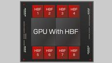
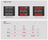 Micron is not alone in exploring this idea. For example, SK hynix and Sandisk have already standardized High-Bandwidth Flash (HBF) as a concept to extend the memory of a GPU's HBM space by bringing NAND closer and offering more durable NAND. Every company working on this idea would need to overcome the bandwidth and durability gap so that HBF or near-GPU NAND becomes a valuable complement to standard HBM memory.
Source:
DigiTimes
For instance, this would enable a GPU to access a potential storage pool with hundreds of gigabytes of storage directly on the GPU package or PCB, similar to what DRAM like HBM or GDDR7/LPDDR6 already does. This tier would sit between GPU memory and regular system storage, acting as a very fast buffer, which would be ideal for the inference of massive LLMs. At that point, LLMs wouldn't be memory-bound and could run on systems with fewer GPUs, but with more storage and memory tiers to compensate for the required inference size. Additionally, this NAND would be significantly cheaper than HBM or regular DRAM and would be sized according to system specifications. Images below are HBF slides from SK hynix and Sandisk.


10 Comments on Micron Explores Near-GPU NAND Flash to Run Bigger LLMs
(source: Samsung's presentation at Hot Chips 2026)
With the HBM base die becoming a full-fledged chiplet, potentially with on-die compute, and manufactured on bleeding edge processes maybe HBF can be chained after HBM. On-die compute or the HBM controller could implement some magical caching scheme using HBF as bulk storage.
Regarding specialized AI GPUs : we already have specialized data center and workstation GPUs tailored for AI , so I don’t think this would change much.
I wonder what the die area would be needed for both the device as well as the phy/controller needed for such thing.
You'd never fly a real CPU with a perishable low-lifetime failure-prone component like this on-chip, it's a warranty and part exchange nightmare waiting to happen, even less for a database server that needs the utmost reliability and lifetime or several years.
Micron should use their profits from DRAM to build a ReRam foundry.
ReRam has the endurance. ReRam is heat tolerant.
That is the future.