Monday, September 7th 2026

Samsung Foundry Allocates Half of 4 nm Capacity for HBM4 Base Dies
According to Korean media, Samsung Foundry, a division that operates silicon manufacturing as a subsidiary of Samsung Electronics, is reportedly allocating significant capacity for HBM4 base die manufacturing. For HBM4, Samsung is producing the base die on a 4 nm node, which reportedly receives half of the entire manufacturing capacity of the 4 nm node, internally referred to as SF4. Customers of HBM4 and the upcoming HBM4E memory standards are now requesting base dies to be filled with custom logic. For instance, customers could implement custom logic like memory controllers and PHYs directly on the HBM base die, significantly reducing the area occupied by these components on the main compute chiplet.
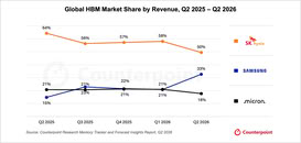
Samsung operates its SF4 manufacturing at Pyeongtaek Campus 2 (P2) and Campus 3 (P3) on lines S5 and S6. An increase in manufacturing is not only coming for ASIC designs by external customers but also for HBM4 base die manufacturing, which is becoming especially important for ASIC customers aiming to maximize the performance of their designs. With its HBM manufacturing business, Samsung is capturing a significant volume from buyers. In Q2 2026, Samsung secured 38% of the HBM market share by revenue, a notable increase from just a year ago when the company held 15%. Meanwhile, SK hynix's share has decreased from 64% in Q2 2025 to 50% in Q2 2026, as many customers have diversified and started sourcing their HBM from Samsung. With more offerings like custom base dies and capacity expansions, Samsung could capture even greater revenue share in the coming quarters if the foundry business continues to perform well.
Sources:
ZDNet Korea, via Jukan on X
Samsung operates its SF4 manufacturing at Pyeongtaek Campus 2 (P2) and Campus 3 (P3) on lines S5 and S6. An increase in manufacturing is not only coming for ASIC designs by external customers but also for HBM4 base die manufacturing, which is becoming especially important for ASIC customers aiming to maximize the performance of their designs.


3 Comments on Samsung Foundry Allocates Half of 4 nm Capacity for HBM4 Base Dies