News Posts matching #EUV

Return to Keyword Browsing

TSMC Completes 5 nm Design Infrastructure, Paving the Way for Silicon Advancement

TSMC announced they've completed the infrastructure design for the 5 nm process, which is the next step in silicon evolution when it comes to density and performance. TSMC's 5 nm process will leverage the company's second implementation of EUV (Extreme Ultra Violet) technology (after it's integrated in their 7 nm process first), allowing for improved yields and performance benefits.

According to TSMC, the 5 nm process will enable up to 1.8x the logic density of their 7 nm process, a 15% clock speed gain due to process improvements alone on an example Arm Cortex-A72 core, as well as SRAM and analog circuit area reduction, which means higher number of chips per wafer. The process is being geared for mobile, internet, and high performance computing applications. TSMC also provides online tools for silicon design flow scenarios that are optimized for their 5 nm process. Risk production is already ongoing.
TSMC 7nm EUV Process to Enter Mass-Production in March 2019

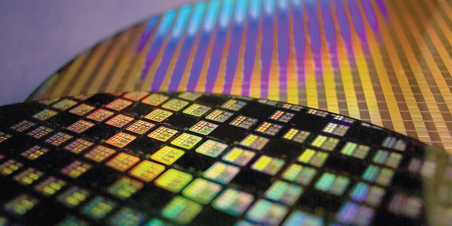
TSMC is giving final touches to set its flagship 7 nanometer EUV (extreme ultraviolet lithography) silicon fabrication node at its highest state of readiness for business, called mass-production. At this state, the node can mass-produce products for TSMC's customers. TSMC had taped out its first 7 nm EUV chips in October 2018. The company will also begin risk-production of the more advanced 5 nm node in April, staying on schedule. Mass production of 5 nm chips could commence in the first half of 2020.

The 7 nm EUV node augments TSMC's 7 nm DUV (deep ultraviolet lithography) node that's been already active since April 2018, and producing chips for AMD, Apple, HiSilicon, and Xilinx. At the turn of the year, 7 nm DUV made up 9 percent of TSMC's shipments. With the new node going online, 7 nm (DUV + EUV) could make up 25 percent of TSMC's output by the end of 2019.

NVIDIA to Implement 7nm EUV Node for its 2020 GPUs

NVIDIA will implement the 7 nanometer EUV (extreme ultraviolet) lithography to build its future generation of GPUs slated for 2020, according to Japanese publication MyNavi.jp. The GPU giant could be among the first customers besides IBM, to contract Samsung for 7 nm EUV mass-production of GPUs. IBM will use the Korean semiconductor giant for manufacturing Z-series processors and FPGAs. Samsung announced in October 2018 that it will begin risk-production on its 7 nm EUV node in early-2019.

An earlier report from 2018 also forecast NVIDIA implementing 7 nm DUV (deep ultraviolet) node of TSMC for its 2019 GPU lineup. With news of the company now working with Samsung on 7 nm EUV for 2020, this seems less likely. It's possible that NVIDIA could somehow split its next generation GPU lineup between TSMC 7 nm DUV and Samsung 7 nm EUV, with the latter being used for chips with higher transistor-counts, taking advantage of the node's higher deliverable transistor densities.

IBM Expands Strategic Partnership with Samsung to Include 7nm Chip Manufacturing

IBM today announced an agreement with Samsung to manufacture 7-nanometer (nm) microprocessors for IBM Power Systems , IBM Z and LinuxONE , high-performance computing (HPC) systems, and cloud offerings. The agreement combines Samsung's industry-leading semiconductor manufacturing with IBM's high-performance CPU designs. This combination is being designed to drive unmatched systems performance, including acceleration, memory and I/O bandwidth, encryption and compression speed, as well as system scaling. It positions IBM and Samsung as strategic partners leading the new era of high-performance computing specifically designed for AI.

"At IBM, our first priority is our clients," said John Acocella, Vice President of Enterprise Systems and Technology Development for IBM Systems. "IBM selected Samsung to build our next generation of microprocessors because they share our level of commitment to the performance, reliability, security, and innovation that will position our clients for continued success on the next generation of IBM hardware."

Intel Unveils a Clean-slate CPU Core Architecture Codenamed "Sunny Cove"

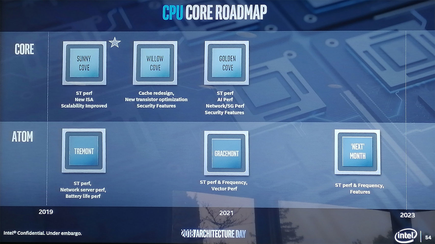
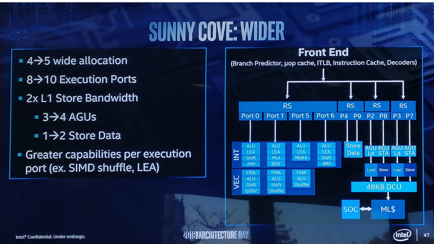
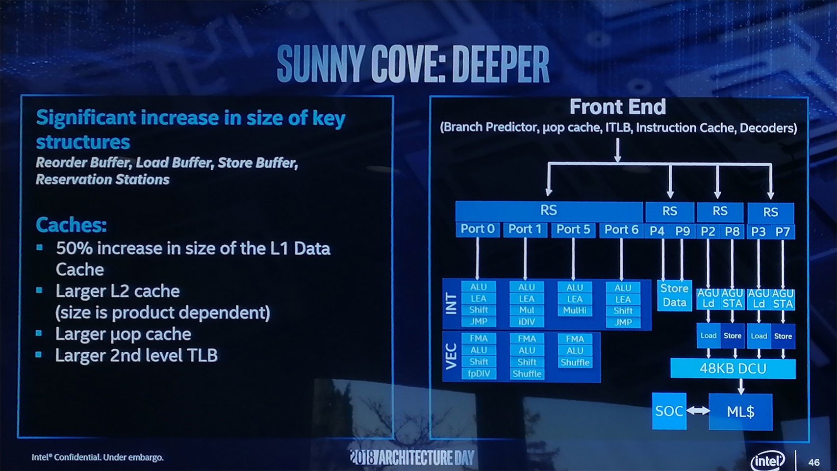
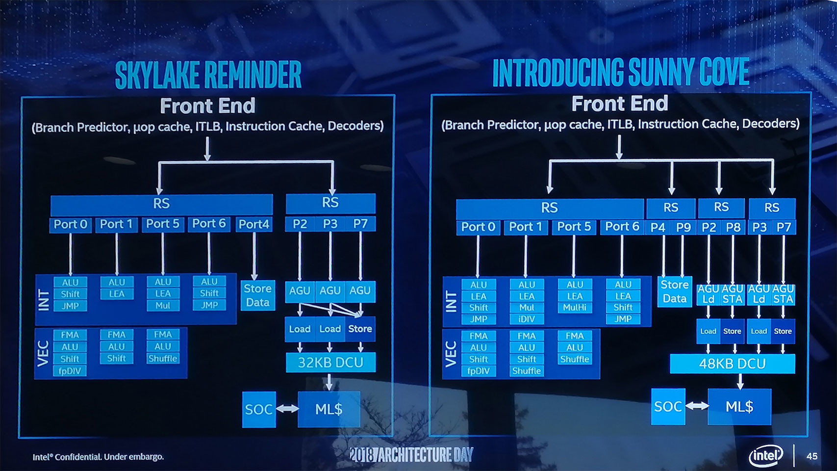
Intel today unveiled its first clean-slate CPU core micro-architecture since "Nehalem," codenamed "Sunny Cove." Over the past decade, the 9-odd generations of Core processors were based on incrementally refined descendants of "Nehalem," running all the way down to "Coffee Lake." Intel now wants a clean-slate core design, much like AMD "Zen" is a clean-slate compared to "Stars" or to a large extent even "Bulldozer." This allows Intel to introduce significant gains in IPC (single-thread performance) over the current generation. Intel's IPC growth curve over the past three micro-architectures has remained flat, and only grew single-digit percentages over the generations prior.

It's important to note here, that "Sunny Cove" is the codename for the core design. Intel's earlier codenaming was all-encompassing, covering not just cores, but also uncore, and entire dies. It's up to Intel's future chip-designers to design dies with many of these cores, a future-generation iGPU such as Gen11, and a next-generation uncore that probably integrates PCIe gen 4.0 and DDR5 memory. Intel details "Sunny Cove" as far as mentioning IPC gains, a new ISA (new instruction sets and hardware capabilities, including AVX-512), and improved scalability (ability to increase core-counts without running into latency problems).

Intel 7nm EUV Node Back On Track, 2x Transistor Densities Over 10nm

There could be light at the end of the tunnel for Intel's silicon fabrication business after all, as the company reported that its 7 nanometer silicon fabrication node, which incorporates EUV (extreme ultraviolet) lithography, is on track. The company stressed in its Nasdaq Investors' Conference presentation that its 7 nm EUV process is de-linked from its 10 nm DUV (deep ultraviolet) node, and that there are separate teams working on their development. The 10 nm DUV node is qualitatively online, and is manufacturing small batches of low-power mobile "Cannon Lake" Core processors.

Cannon Lake is an optical shrink of the "Skylake" architecture to the 10 nm node. Currently there's only one SKU based on it, the Core i3-8121U. Intel utilized the electrical gains from the optical shrink to redesign the client-segment architecture's FPU to support the AVX-512 instruction-set (although not as feature-rich as the company's enterprise-segment "Skylake" derivatives). The jump from 10 nm DUV to 7 nm EUV will present a leap in transistor densities, with Intel expecting nothing short of a doubling. 10 nm DUV uses a combination of 193 nm wavelength ultraviolet lasers and multi-patterning to achieve its transistor density gains over 14 nm++. The 7 nm EUV node uses an extremely advanced 135 nm indirect laser, reducing the need for multi-patterning. The same laser coupled with multi-patterning could be Intel's ticket to 5 nm.

Samsung Electronics Starts Production of EUV-based 7nm LPP Process

Samsung Electronics, a world leader in advanced semiconductor technology, today announced that it has completed all process technology development and has started wafer production of its revolutionary process node, 7LPP, the 7-nanometer (nm) LPP (Low Power Plus) with extreme ultraviolet (EUV) lithography technology. The introduction of 7LPP is a clear demonstration of Samsung Foundry's technology roadmap evolution and provides customers with a definite path to 3nm. The commercialization of its newest process node, 7LPP gives customers the ability to build a full range of exciting new products that will push the boundaries of applications such as 5G, Artificial Intelligence, Enterprise and Hyperscale Datacenter, IoT, Automotive, and Networking.

"With the introduction of its EUV process node, Samsung has led a quiet revolution in the semiconductor industry," said Charlie Bae, executive vice president of foundry sales and marketing team at Samsung Electronics. "This fundamental shift in how wafers are manufactured gives our customers the opportunity to significantly improve their products' time to market with superior throughput, reduced layers, and better yields. We're confident that 7LPP will be an optimal choice not only for mobile and HPC, but also for a wide range of cutting-edge applications."

TSMC to be the Sole Supplier of Apple A13 SoCs in 2019

Even as AMD plans to dedicate 7 nm CPU and GPU manufacturing entirely to TSMC, reports are emerging that Apple could make the Taiwanese silicon fabrication giant the sole supplier of its 7 nm A13 SoC, which powers the next generation iPhone and iPad devices. Manufacturing of the A13 could commence in 2019 to keep pace with Apple's roadmaps. TSMC is currently the most strongly placed semiconductor foundry for 7 nm EUV manufacturing, after GlobalFoundries crashed out, and Samsung is trailing behind with a contract to manufacture only a portion of Qualcomm's next-generation Snapdragon SoCs.

TSMC Increases Industry Foothold With 11.6% Increase in Revenue for Q3 2018

TSMC has quickly (over a span of years, but still) become the de-facto silicon manufacturing giant in the industry. They produce silicon-based solutions for almost all the significant tech companies (NVIDIA, AMD, Apple, Qualcomm, including the silicon manufacturing leader of yonder, Intel), and are on the forefront of new fabrication technologies. Just today we've covered how they are already well on their way to their second-gen 7 nm (N7+) fabrication technology with usage of EUV, and carving their path forward for 5 nm (N5).

TSMC 7 nm Second-Generation EUV Chips Taped Out, 5 nm Risk Production in April 2019

TSMC, the world's biggest contract semiconductor manufacturer, who is at the forefront of 7 nanometer production has just announced that they are making good progress with their second generation of 7 nm technology "N7+", using EUV (Extreme Ultraviolet Lithography). A first design for N7+ from an unnamed customer has been taped out. The company's first-gen 7 nm production is running well already, with final products, like Apple iPhone already in the hands of customers.

While not fully EUV yet, the N7+ process will see limited EUV usage, for up to four non-critical layers, which gives the company an opportunity to figure out how to make best use of the new technology, how to ramp up for mass production and how to fix the little quirks that show up as soon as you move from the lab to the factory.

Analyst Firm Susquehanna: "Intel Lost its Manufacturing Leadership"

Intel was once the shining star in the semiconductor manufacturing industry, with a perfectly integrated, vertical product design and manufacturing scheme. Intel was one of the few companies in the world to be able to both develop its architectures and gear their manufacturing facilities to their design characteristics, ensuring a perfect marriage of design and manufacturing. However, not all is rosy on that field, as we've seen; AMD itself also was a fully integrated company, but decided to spin-off its manufacturing arm so as to survive - thus creating GLOBALFOUNDRIES.But Intel was seen as many as the leader in semiconductor manufacturing, always at the cutting edge of - well - Moore's Law, named after Intel's founding father Gordon Moore. Now, Mehdi Hosseini, an analyst with Susquehanna, has gone on to say that the blue giant has effectively lost its semiconductor leadership. And it has, in a way, even if its 10 nm (which is in development hell, so to speak) is technically more advanced than some 7 nm implementations waiting to be delivered to market by its competitors. However, there's one area where Intel will stop being able to claim leadership: manufacturing techniques involving EUV (Extreme UltraViolet).

Challenges With 7 nm, 5 nm EUV Technologies Could Lead to Delays In Process' TTM

Semiconductor manufacturers have been historically bullish when it comes to the introduction of new manufacturing technologies. Intel, AMD (and then Globalfoundries), TSMC, all are companies who thrive in investors' confidence: they want to paint the prettiest picture they can in terms of advancements and research leadership, because that's what attracts investment, and increased share value, and thus, increased funds to actually reach those optimistic goals.

However, we've seen in recent years how mighty Intel itself has fallen prey to unforeseen complications when it comes to advancements of its manufacturing processes, which saw us go from a "tick-tock" cadence of new architecture - new manufacturing process, to the introduction of 14 nm ++ processes. And as Intel, Globalfoundries and TSMC race towards sub 7-nm manufacturing processes with 250 mm wafers and EUV usage, things aren't getting as rosy as the ultraviolet moniker would make us believe.

Samsung Electronics Breaks Ground on a New EUV Line

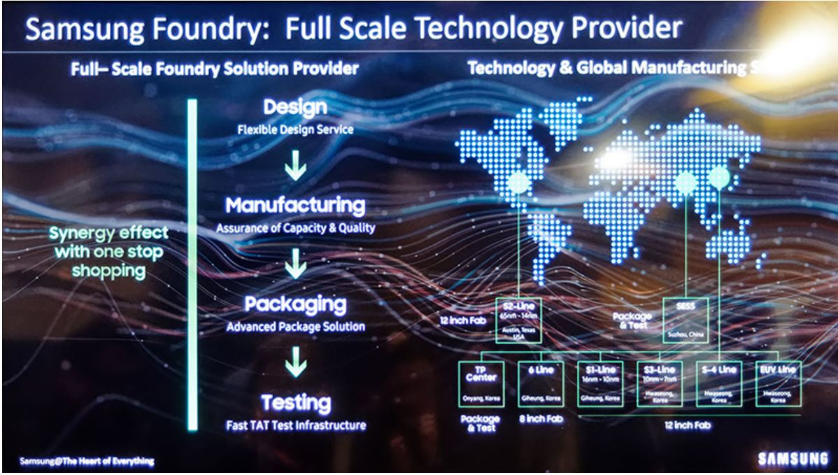
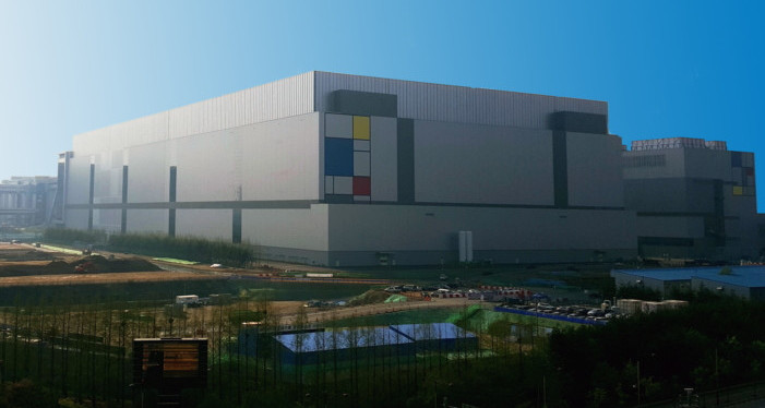
Samsung Electronics Co., Ltd., a world leader in advanced semiconductor technology, today broke ground on a new EUV (extreme ultraviolet) line in Hwaseong, Korea, aiming to maintain its leadership in state-of-the-art semiconductor technology. With this new EUV line, Samsung will be able to strengthen its leadership in the single nanometer process technology by responding to market demand from various applications, including mobile, server, network, and HPC (high performance computing), where high performance and power efficiency are critical.

The new facility is expected to be completed within the second half of 2019 and start production ramp-up in 2020. The initial investment in this new EUV line is projected to reach US$ 6 billion by 2020 and additional investment will be determined depending on market circumstances. Samsung has decided to utilize cutting-edge EUV technology starting with its 7-nanometer (nm) LPP (Low Power Plus) process. This new line will be set up with EUV lithography equipment to overcome nano-level technology limitations. Samsung has continued to invest in EUV R&D to support its global customers for developing next-generation chips based on this leading-edge technology.

Qualcomm to Build Snapdragon 5G SoCs on Samsung 7nm LPP EUV Process

Samsung Electronics, a world leader in advanced semiconductor technology, and Qualcomm Technologies, Inc., a subsidiary of Qualcomm Incorporated, today announced the intention to expand their decade-long foundry relationship into EUV (extreme ultra violet) lithography process technology, including the manufacture of future Qualcomm Snapdragon 5G mobile chipsets using Samsung's 7-nanometer (nm) LPP (Low Power Plus) EUV process technology.

Using 7LPP EUV process technology, Snapdragon 5G mobile chipsets will offer a smaller chip footprint, giving OEMs more usable space inside upcoming products to support larger batteries or slimmer designs. Process improvements, combined with a more advanced chip design, are expected to bring significant improvements in battery life.

TSMC to Build World's First 3 nm Fab in Taiwan

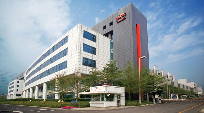
TSMC has announced the location for their first 3 nm fab: it will be built in the Tainan Science Park, southern Taiwan. Rumors pegged the new 3 nm factory as possibly being built in the US, due to political reasons; however, TSMC opted to keep their production capabilities clustered in the Tainan Science Park, where they can better leverage their assets and supply chain for the production and support of the world's first 3 nm semiconductor factory. It certainly also helped the Taiwanese government's decision to pledge land, water, electricity and environmental protection support to facilitate TSMC's latest manufacturing plan. It's expected that at least part of the manufacturing machines will be provided by ASML, a Netherlands-based company which has enjoyed 25% revenue growth already just this year.

As part of the announcement, TSMC hasn't given any revised timelines for their 3 nm production, which likely means the company still expects to start 3 nm production by 2022. TSMC said its 7 nm yield is ahead of schedule, and that it expects a fast ramp in 2018 - which is interesting, considering the company has announced plans to insert several extreme ultraviolet (EUV) layers at 7 nm. TSMC has also said its 5 nm roadmap is on track for a launch in the first quarter of 2019.

AMD to Build "Zen 2" and "Zen 3" Processors on 7 nm Process: CTO

AMD is in no mood to stick to the 14 nm process for as long as Intel has (building four performance x86 CPU micro-architectures on it). In an interview with EE Times, AMD CTO Mark Papermaster confirmed that the company's "Zen 2" and "Zen 3" CPU micro-architectures will be built on the next-generation 7 nm silicon fab process. Transition to the 7 nm process is not as straightforward as optically shrinking your chip designs and shipping them over to your foundry. Apparently it requires big technical changes for the chip design teams, which AMD feels are better executed while it's still riding on the success of its current "Zen" architecture.

"We had to literally double our efforts across foundry and design teams…It's the toughest lift I've seen in a number of generations," said Papermaster. He added that the 7 nm node requires new "CAD tools and [changes in] the way you architect the device [and] how you connect transistors-the implementation and tools change [as well as] the IT support you need to get through it." Papermaster predicts that 7 nm will be a "long node like 28 nm" in that chip designers will have to build several refinements to their designs on the node before the newer 4 nm node could be heralded. He urged semiconductor foundry companies to introduce EUV (extreme ultra-violet lithography), a technique used to etch transistors and circuits at the infinitesimally small 7 nm node, as soon as possible, so AMD could have more options at manufacturing its next generation processors.

Demand for EUV Fabrication Systems Increasing; ASML Sees 25% Revenue Growth

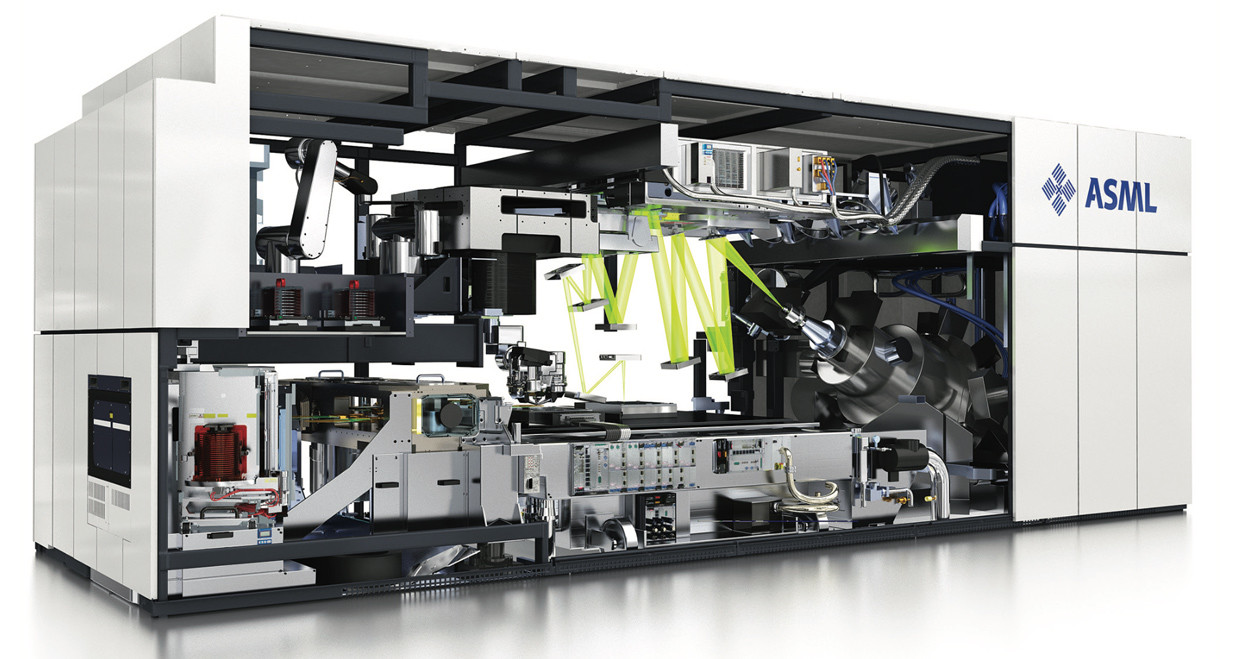
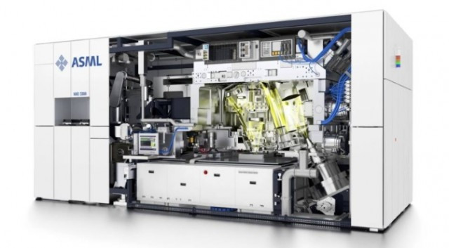
Dutch company ASML may not be very known to us mortal users, but it has one of the greatest aces up its sleeve: it specializes in what are some of the most complex machines currently made by mankind. Extreme Ultraviolet Lithography Systems (EUV) are the kind of machines that make you look in wonder and amazement at man's ingenuity - ASML, which specializes in this type of systems, has a production capability for 2017 that numbers just 12 of these. That means on average, they take a whole month putting one of these together. That really goes to show the complexity inherent to these systems. And it shows: EUV machines are about the size of a city bus, and typically cost more than 100 million euros ($115.3 million) each.

The revenue growth forecast is spurred by an additional 8 EUV systems being ordered by ASML's clients, which include Intel, Samsung, and TSMC - some of the biggest players in the semiconductor business. The new orders brought the company's order backlog to 27 machines - more than double their current annual output. ASML is taking steps to to ensure an increase in production capability to keep up with the multi million-dollar demand: the company is set to expand its system production capability to 24 in 2018, before reaching an expected capacity of around 40 systems in 2019. Third-quarter revenue will be about 2.2 billion euros ($2.5 billion), the Veldhoven, Netherlands-based maker of chip-making machines predicts. The company's stock valuation has increased some 30% over the past year - the company's valuation currently stands at around €53 billion ($61 billion.)

IBM Research Alliance Builds New Transistor for 5 nm Technology

IBM, its Research Alliance partners GLOBALFOUNDRIES and Samsung, and equipment suppliers have developed an industry-first process to build silicon nanosheet transistors that will enable 5 nanometer (nm) chips. The details of the process will be presented at the 2017 Symposia on VLSI Technology and Circuits conference in Kyoto, Japan. In less than two years since developing a 7 nm test node chip with 20 billion transistors, scientists have paved the way for 30 billion switches on a fingernail-sized chip.

The resulting increase in performance will help accelerate cognitive computing, the Internet of Things (IoT), and other data-intensive applications delivered in the cloud. The power savings could also mean that the batteries in smartphones and other mobile products could last two to three times longer than today's devices, before needing to be charged.

Samsung Announces Comprehensive Process Roadmap Down to 4 nm

Samsung stands as a technology giant in the industry, with tendrils stretching out towards almost every conceivable area of consumer, prosumer, and professional markets. It is also one of the companies which can actually bring up the fight to Intel when it comes to semiconductor manufacturing, with some analysts predicting the South Korean will dethrone Intel as the top chipmaker in Q2 of this year. Samsung scales from hyper-scale data centers to the internet-of-things, and is set to lead the industry with 8nm, 7nm, 6nm, 5nm, 4nm and 18nm FD-SOI in its newest process technology roadmap. The new Samsung roadmap shows how committed the company is (and the industry with it) towards enabling the highest performance possible from the depleting potential of the silicon medium. The 4 nm "post FinFET" structure process is set to be in risk production by 2020.

This announcement also marks Samsung's reiteration on the usage of EUV (Extreme Ultra Violet) tech towards wafer manufacturing, a technology that has long been hailed as the savior of denser processes, but has been ultimately pushed out of market adoption due to its complexity. Kelvin Low, senior director of foundry marketing at Samsung, said that the "magic number" for productivity (as in, with a sustainable investment/return ratio) with EUV is 1,500 wafers per day. Samsung has already exceeded 1,000 wafers per day and has a high degree of confidence that 1,500 wafers per day is achievable.

Samsung Details New Foundry Offerings at 14nm (LPU) and 10nm (LPU)

In an announcement that's sure to stir the foundry gods, Samsung Electronics, a world leader in advanced semiconductor technology, announced today that it is expanding its advanced foundry process technology offerings with the fourth-generation 14-nanometer (nm) process (14LPU) and the third-generation 10nm process (10LPU). The announcement comes as Samsung increases investment so as to meet the requirements of next generation products, ranging from mobile and consumer electronics (Snapdragon 830 and Samsung's own Exynos 8895 come to mind) to data centers and automotives.

Ben Suh, Senior Vice President of foundry marketing at Samsung Electronics, issued the following statement: "After we announced the industry's first 10nm mass production in mid-October, we have now also expanded our lineup with new foundry offerings, 14LPU and 10LPU. Samsung is very confident with our technology definitions that provide design advantages on an aggressive process with manufacturability considerations. We have received tremendous positive market feedback and are looking forward to expanding our leadership in the advanced process technology space."
Return to Keyword Browsing
Nov 11th, 2026 07:09 CST change timezone

New Forum Posts

Popular Reviews

TPU on YouTube

Controversial News Posts