Tuesday, October 3rd 2017

TSMC to Build World's First 3 nm Fab in Taiwan

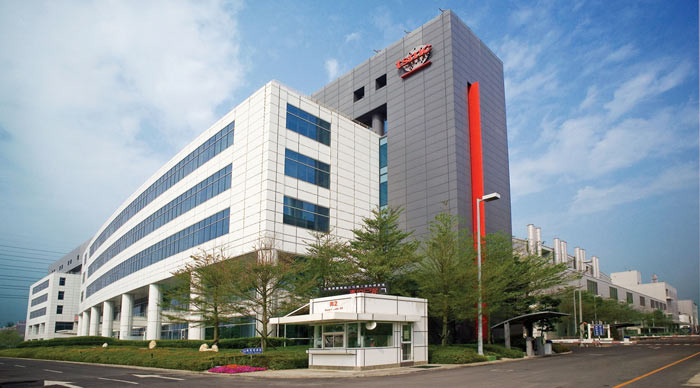
TSMC has announced the location for their first 3 nm fab: it will be built in the Tainan Science Park, southern Taiwan. Rumors pegged the new 3 nm factory as possibly being built in the US, due to political reasons; however, TSMC opted to keep their production capabilities clustered in the Tainan Science Park, where they can better leverage their assets and supply chain for the production and support of the world's first 3 nm semiconductor factory. It certainly also helped the Taiwanese government's decision to pledge land, water, electricity and environmental protection support to facilitate TSMC's latest manufacturing plan. It's expected that at least part of the manufacturing machines will be provided by ASML, a Netherlands-based company which has enjoyed 25% revenue growth already just this year.

As part of the announcement, TSMC hasn't given any revised timelines for their 3 nm production, which likely means the company still expects to start 3 nm production by 2022. TSMC said its 7 nm yield is ahead of schedule, and that it expects a fast ramp in 2018 - which is interesting, considering the company has announced plans to insert several extreme ultraviolet (EUV) layers at 7 nm. TSMC has also said its 5 nm roadmap is on track for a launch in the first quarter of 2019.
Sources: EETimes, Tweakers.net, Thanks @ P4-630!
Add your own comment

18 Comments on TSMC to Build World's First 3 nm Fab in Taiwan

#1
Prima.Vera
Congrats! Is interesting to see that the GPUs will be way ahead of CPUs from technology point of view.
Also, isn't AMD using TSMC?
Posted on Reply
#2
Melvis
Prima.VeraAlso, isn't AMD using TSMC?
That's what I was also thinking.
Posted on Reply
#4
ratirt
3nm damn. Wonder what would be next. 1nm ? I thought Moor's law is reaching it's "impossible to go any smaller" and here we'll have 3nm fabs.
Posted on Reply
#5
Nokiron
ratirt3nm damn. Wonder what would be next. 1nm ? I thought Moor's law is reaching it's "impossible to go any smaller" and here we'll have 3nm fabs.
That's not what Moore's Law is saying.
Posted on Reply
#6
bug
ratirt3nm damn. Wonder what would be next. 1nm ? I thought Moor's law is reaching it's "impossible to go any smaller" and here we'll have 3nm fabs.
Impossible to go smaller isn't about Moore's law, it's about physics. And that limit is approaching fast. I've seen it estimated at ~5nm (which is apparently wrong), but it can't be too far away. And the simple explanation is at that size, there are only a handful of atoms in a transistor (the radius of the Si atom is about 100pm) which can't hold much of an electrical charge.
Posted on Reply
#7
Frick
Fishfaced Nincompoop
bugImpossible to go smaller isn't about Moore's law, it's about physics. And that limit is approaching fast. I've seen it estimated at ~5nm (which is apparently wrong), but it can't be too far away. And the simple explanation is at that size, there are only a handful of atoms in a transistor (the radius of the Si atom is about 100pm) which can't hold much of an electrical charge.
There's also the matter of how you measure, and about that I can tell you nothing.
FreedomEclipseFab-u-loussssssssss
Like AMD. :p
Posted on Reply
#8
Shamalamadingdong
Or more accurately they're about to build the world's first 3* nm fab.

*Not actually 3 nm.
Posted on Reply
#9
Prima.Vera
bugImpossible to go smaller isn't about Moore's law, it's about physics. And that limit is approaching fast. I've seen it estimated at ~5nm (which is apparently wrong), but it can't be too far away. And the simple explanation is at that size, there are only a handful of atoms in a transistor (the radius of the Si atom is about 100pm) which can't hold much of an electrical charge.
Is OK, physics is not an issue. The actual technology is, but that is improving a lot as well. In the future is even possible to go on the quantum level, 1 atom = 1 transistor, but we are at least 50 years from that. Don't worry, why do you think ALL of the biggest companies are investing so hugely in Artificial Intelligence? A powerful enough computer, can design new technical solution and technologies to print out micro conductors and simmilar....
Posted on Reply
#10
bug
Prima.VeraIs OK, physics is not an issue. The actual technology is, but that is improving a lot as well. In the future is even possible to go on the quantum level, 1 atom = 1 transistor, but we are at least 50 years from that. Don't worry, why do you think ALL of the biggest companies are investing so hugely in Artificial Intelligence? A powerful enough computer, can design new technical solution and technologies to print out micro conductors and simmilar....
Or as others have said, the age of man ends when we build the first robot that is able to build a better version of itself ;)
Posted on Reply
#11
Prima.Vera
bugOr as others have said, the age of man ends when we build the first robot that is able to build a better version of itself ;)
You watched too much Hollywood crap, lol!
Posted on Reply
#12
bug
Prima.VeraYou watched too much Hollywood crap, lol!
No, that one is actually sound if think about it.
Posted on Reply
#13
eidairaman1
The Exiled Airman
Well thats a tiny plant.


Joking aside, in more news computers wont't exist after I'm gone as everything will be done by our own brains again lol.
Posted on Reply
#14
Solaris17
Super Dainty Moderator
ShamalamadingdongOr more accurately they're about to build the world's first 3* nm fab.

*Not actually 3 nm.
Thats what I was thinking. Isn't this data skewed? I thought that AMD, Intel, Goflo, TSMC calculated NM differently? I was under the impression thats a game they started playing around 2 years ago.
Posted on Reply
#15
Steevo
bugImpossible to go smaller isn't about Moore's law, it's about physics. And that limit is approaching fast. I've seen it estimated at ~5nm (which is apparently wrong), but it can't be too far away. And the simple explanation is at that size, there are only a handful of atoms in a transistor (the radius of the Si atom is about 100pm) which can't hold much of an electrical charge.
It's less about the ability to hold a charge and more about the quantum tunneling issues of electrons at specific gate insulation thickness. TSMC may be on track to allow smaller actual traces than Intel, due to the way their measurements work at this level, which is why Ryzen was so power efficient at the clocks it would reach.
Posted on Reply
#16
bug
SteevoIt's less about the ability to hold a charge and more about the quantum tunneling issues of electrons at specific gate insulation thickness. TSMC may be on track to allow smaller actual traces than Intel, due to the way their measurements work at this level, which is why Ryzen was so power efficient at the clocks it would reach.
Potayto - potahto. When electrons tunnel, the charge goes away.
But your description describes what happens more accurately.
Posted on Reply
#17
Psinet
Intel: What is this?

SEMICONDUCTORS FOR ANTS??!
Posted on Reply
#18
Kanan
Tech Enthusiast & Gamer
Solaris17Thats what I was thinking. Isn't this data skewed? I thought that AMD, Intel, Goflo, TSMC calculated NM differently? I was under the impression thats a game they started playing around 2 years ago.
It's skewed because TSMC and GloFo started using marketing terms for their 20nm approach ("16"/"14"nm) to pretend they are not that far behind Intel, or even on same level, because they simply aren't and that's bad, basically meaning they are not on track. 14nm Intel tech is far smaller and more advanced, 16/14nm of those other companies is basically only 20nm production.
Prima.VeraCongrats! Is interesting to see that the GPUs will be way ahead of CPUs from technology point of view.
Also, isn't AMD using TSMC?
And for the same reason, this is wrong. Intel will still be ahead, I can only see Samsung doing a big move, but not TSMC.
Posted on Reply
Add your own comment
Apr 27th, 2024 16:21 EDT change timezone

New Forum Posts

Popular Reviews

Controversial News Posts