Wednesday, April 11th 2018
Challenges With 7 nm, 5 nm EUV Technologies Could Lead to Delays In Process' TTM
Semiconductor manufacturers have been historically bullish when it comes to the introduction of new manufacturing technologies. Intel, AMD (and then Globalfoundries), TSMC, all are companies who thrive in investors' confidence: they want to paint the prettiest picture they can in terms of advancements and research leadership, because that's what attracts investment, and increased share value, and thus, increased funds to actually reach those optimistic goals.
However, we've seen in recent years how mighty Intel itself has fallen prey to unforeseen complications when it comes to advancements of its manufacturing processes, which saw us go from a "tick-tock" cadence of new architecture - new manufacturing process, to the introduction of 14 nm ++ processes. And as Intel, Globalfoundries and TSMC race towards sub 7-nm manufacturing processes with 250 mm wafers and EUV usage, things aren't getting as rosy as the ultraviolet moniker would make us believe.
 Expectations may well be on their way to a bearish correction in estimates, as new research - and actual silicon production - has come to put to question previously estimated timelines for 7 nm and 5 nm products. The issue with 7 nm is a lighter one - yields aren't where manufacturers want to be as of yet. But that's expected (even if they're worse than expected) and there's still time to improve yields until actual product launches (such as AMD's Zen 2, for example). However, at 5 nm, things are getting too small for current process technology - defects and yields are way below expected levels, with various different anomalies cropping up in test production. And just consider the economics of actually finding the defects: researchers are being quoted as taking days to scan 7 nm and 5 nm-class chips for defects.
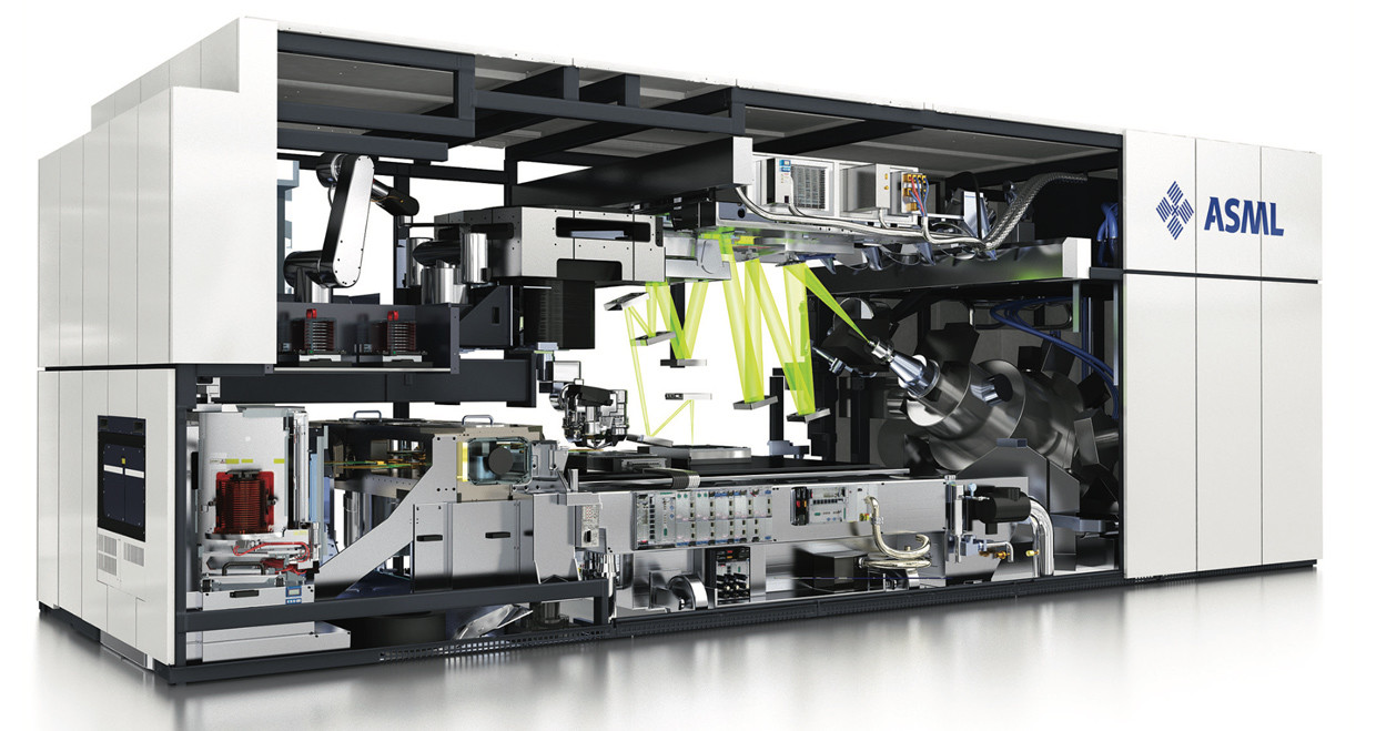
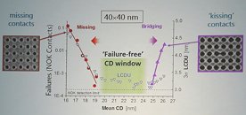 These are cropping up at critical dimensions around 15 nm, needed to make 5 nm chips for foundry processes (which were targeting 2020 for actual production). EUV-machine maker ASML is now reportedly preparing a new, next-generation EUV system that actually deals with these finer printing defects - but those systems aren't expected to be available until 2024.
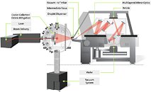 There's just another slight quibble with the whole new EUV production process, though: the base physics behind it. The fact remains that researchers and engineers still don't understand exactly what interactions are relevant, and occurring, in the etching of these so extremely fine patterns with EUV lighting. You'd expect some unforeseen problems arising, then, and the need for further study, trial and error, and iteration, just to understand those interactions that end up affecting final wafer quality. There goes the 2020 window, it seems.
Source:
EETimes Asia
However, we've seen in recent years how mighty Intel itself has fallen prey to unforeseen complications when it comes to advancements of its manufacturing processes, which saw us go from a "tick-tock" cadence of new architecture - new manufacturing process, to the introduction of 14 nm ++ processes. And as Intel, Globalfoundries and TSMC race towards sub 7-nm manufacturing processes with 250 mm wafers and EUV usage, things aren't getting as rosy as the ultraviolet moniker would make us believe.


11 Comments on Challenges With 7 nm, 5 nm EUV Technologies Could Lead to Delays In Process' TTM
It was never a question to me whether we'd read this someday, more a question of when :D
Well, there's your problem
www.spiedigitallibrary.org/conference-proceedings-of-spie/10584/2299644/Overlay-improvements-using-a-novel-high-order-distortion-correction-system/10.1117/12.2299644.short
"Throughputs of up to 90 wafers per hour were achieved.." - March 19, 2018
This is compared to EUVL from July 2017; "The NXE:3400B scanner exposed 104 WPH at 148 W "
EUV and NIL tied out mostly between the industry; leaning in EUVs favor.
Canon and Dai Nippon are Intel partners. So, NIL might be the post Immersion Litho for Intel. They have the partnership, etc.
electroiq.com/blog/2016/02/yield-and-cost-challenges-at-16nm-and-beyond/
Notice the big increase from 20 nm and up. When you have much more steps to deal with, the potential of having flaws increases as well.
This graph shows how yields would become if they stayed constant @ 28 nm numbers: as seen, they go from just shy of 80% @ 28 nm to around 56% @ 5 nm. Obviously, the manufacturing process improves over time so the yields also improve but the pic shows how much of an obstacle it is to adopt newer process sizes.
Besides, and before that, you need to have people in R&D that know all the ins and outs of carbon nanotubes, and we still haven't discovered everything about them. So, I'd say it would take ten years more at least before we see them in everyday technologies.