News Posts matching #UV

Return to Keyword Browsing

Samsung Electronics and ASML Expand Collaboration for Next-Generation Semiconductor Manufacturing

Samsung Electronics and ASML today announced an expansion of their long-standing strategic partnership, deepening collaboration on High NA EUV lithography and advanced semiconductor manufacturing technologies that will help drive the next generation of innovation in the AI era.

Building on years of successful cooperation, the companies will work together to accelerate the development and deployment of technologies that support the increasing performance and efficiency requirements of advanced semiconductor manufacturing.

TSMC and ASML Announce Initiative to Pioneer Industry Transition to Large-Format Photomasks for High NA EUV

ASML Holding N.V. (Euronext: ASML, Nasdaq: ASML) and Taiwan Semiconductor Manufacturing Company (TWSE: 2330, NYSE: TSM) announced a collaborative initiative to lead the semiconductor industry's transition to a larger-format Extreme Ultraviolet (EUV) lithography photomask.

While High NA EUV will be adopted for production using the current, 6-inch masks, the transition to larger, 12-inch masks is expected to further increase fab productivity, lower chipmaking costs and remove stitching constraints, benefiting the entire semiconductor industry. It will enable advanced chip manufacturers to fully leverage the advantages of High NA EUV, making future generations of leading-edge chips more cost-effective.

Lam Research Announces Plans to Invest More than $3B to Expand Global Lab Network

Lam Research Corp. (NASDAQ: LRCX) today announced that it intends to invest more than $3 billion over the next five years to expand its global research and development (R&D) lab network. The planned multi-site expansion is expected to add infrastructure and capabilities to increase experiment capacity by more than 50%. Lam's R&D approach combines specialized labs worldwide, each purpose-built to accelerate a distinct step of the innovation cycle, with deep customer collaboration that includes locations near customer facilities. Together, Lam's labs operate as an integrated 24/7 network, enabling innovation in parallel and at scale. With this investment, Lam intends to further compress product development cycles for customers, from pathfinding to fab deployment.

"In the AI era, the pace of innovation is relentless, requiring chips with new architectures, different materials, and complex features engineered with nanoscale precision. Our ability to increase velocity throughout the R&D process has become a decisive advantage," said Tim Archer, president and chief executive officer of Lam Research. "We are investing with the intention of staying ahead of what our customers need, further strengthening our global innovation engine to deliver the next generation of semiconductor breakthroughs."

China Begins Limited Production of Domestic Immersion DUV Machines

According to sources close to The Information, a Chinese company Shanghai Yuliangsheng Technology has reportedly begun limited production of immersion DUV lithography machines. This Shanghai-based company aims to produce five systems for delivery this year, with an estimated production of about 20 immersion DUV machines by 2027. While this may not seem like a large number, it represents a significant effort in developing homegrown DUV machine production, reducing reliance on third-party suppliers like ASML. The Shanghai company plans initial deliveries to SMIC, CXMT, and Hua Hong, which will integrate these machines into their production processes.

For those unfamiliar, immersion deep ultraviolet (DUV) machines use an argon-fluoride (ArF) excimer laser to produce DUV light at a 193 nm wavelength. This light travels through a layer of ultra-purified water placed above the final lens, which imprints circuit designs onto a wafer. Although this may sound straightforward, immersion DUV lithography tools are highly complex machines that ASML has been mass-producing for years. By comparison, ASML shipped 131 immersion DUV machines last year, showing the smaller scale of the Chinese production. Additionally, Chinese immersion DUV also imports some key components from Japan, while most are being sourced from China.

ASML Considers Price Increase for Low-NA EUV, TSMC Unhappy

According to the latest information from the second quarter financial results, ASML is considering raising prices for its Low-NA EUV tools, which is reportedly upsetting its customers. ASML CFO Roger Dassen has noted that the company is looking into price increases for these tools, aligning its pricing strategy with product value. As the company continues to enhance the productivity of its tools, ASML plans to adjust pricing accordingly. The company operates a business unit called Installed Base Management, which focuses on maintaining and improving existing machines. Most of the recent productivity gains have come from ASML's software that operates EUV machines, and the company recently confirmed that:
ASML CFO Roger DassenWhen it comes to Low-NA pricing, of course, you know that we keep on increasing the productivity of the Low-NA tool. Of course, that gives us a pretty strong runway for potential price improvements going forward... Value-based pricing is the concept that we follow within ASML. In the current environment, of course, the value for customers is higher than in other circumstances.

ASML, TSMC, and imec Achieve 300 mm Integration of 2D-Material Transistors with 50 nm Pitch

This week, at the 2026 IEEE/JSAP Symposium on VLSI Technology and Circuits, imec, a world-leading research and innovation hub in advanced semiconductor technologies, in partnership with the lithography solution provider ASML, and semiconductor foundry TSMC, presents a novel, robust and scalable 300 mm integration route for 2D-material based n and pFETs. For the first time, scaled nFETs (implementing MoS2 as the channel material) and pFETs (either WS2 or WSe2-based) with 50 nm contacted poly pitch (CPP) could be demonstrated, with good current-voltage characteristics. These results represent a crucial step in the lab-to-fab transition of 2D-material based transistors, envisioned for ultra-scaled logic as well as for back-end and wafer backside applications.

2D transition metal dichalcogenides (TMDs, such as MoS2, WS2, and WSe2) have the potential to extend and augment the logic scaling technology roadmap. When integrated as atomically thin conduction channels replacing Si, these materials enable high-performance scaled transistors - attractive for ultra-scaled logic as well as for back-end-of-line and wafer backside applications. They owe this promise to their good electrostatic channel control while maintaining acceptable carrier mobilities, even at ultra-scaled gate and channel lengths. But the path to industrial adoption has so far been hampered by the lack of a 300 mm integration route that can offer TMD-based n and pFETs at industry-relevant dimensions, while preserving the performance that has extensively been demonstrated on a lab scale.

Imec Receives the World's Most Advanced High NA EUV System

Today, imec, a world-leading research and innovation hub in advanced semiconductor technologies, announces the arrival of the ASML EXE:5200 High NA EUV lithography system, the most advanced lithography tool available today. With this strategic milestone, imec reinforces its position as the industry's launchpad into the ångström era, giving its global partners ecosystem unparalleled early access to the next generation of chip-scaling technologies. Integrated directly with a comprehensive suite of patterning and metrology tools and materials, the High NA EUV system will empower imec and its ecosystem partners to unlock the performance needed to pioneer sub-2 nm logic and high-density memory technologies that will fuel the rapid growth of advanced AI and high-performance computing.

Luc Van den hove, CEO of imec: "The past two years have marked an important chapter for High NA (0.55NA) EUV lithography, with imec and ASML joining forces with the ecosystem in its joint High NA EUV Lithography Lab in Veldhoven (The Netherlands) to pioneer High NA EUV technology. With the installation of the EXE:5200 High NA EUV lithography system into our 300 mm cleanroom in Leuven (Belgium), we aim to bring these High NA EUV patterning technologies to an industry-relevant scale and to develop the next-generation High NA EUV patterning use cases. Its unmatched resolution, improved overlay performance, high throughput, and a new wafer stocker that improves process stability and throughput, will give our partners a decisive advantage in accelerating the development of sub-2 nm chip technologies. As the industry moves into the ångström era, High NA EUV will be a cornerstone capability, and imec is proud to lead the way by offering its partners the earliest and most comprehensive access to this technology."

IBM and Lam Research Announce Collaboration to Advance Sub-1 nm Logic Scaling

IBM (NYSE: IBM) and Lam Research Corp. (NASDAQ: LRCX) today announced a collaboration aimed at developing new processes and materials to support sub-1 nm logic scaling. Building on a long record of successful partnerships, the new agreement will focus on the joint development of novel materials, fabrication processes, and High-NA EUV lithography processes to advance IBM's logic scaling roadmap.

IBM and Lam have collaborated for more than a decade to advance logic fabrication, notably enabling early generations of 7 nm, nanosheet, and EUV process technologies. Under this new five-year agreement, the companies intend to extend logic scaling to the sub-1 nm node. The work will focus on developing new materials, advanced etch and deposition capabilities for increasingly complex device architectures, and new High-NA EUV lithography processes to enable next-generation interconnect and device patterning and accelerate industry adoption.

ASML Boosts EUV Power to 1,000W for Better Yields and Lower Chip Costs

ASML says it has boosted the light source power in its EUV lithography systems to 1,000 watts, up from roughly 600 W today. According to a Reuters report, the company claims the increase could enable up to 50% more chip output by the end of the decade. More source power translates directly into higher throughput. ASML says customers could process around 330 wafers per hour by 2030, compared to about 220 wafers per hour today, lowering the cost per chip. EUV light at a 13.5 nm wavelength is generated by firing a CO₂ laser at microscopic droplets of molten tin, creating plasma that emits EUV radiation. The light is then collected and directed through precision optics supplied by Carl Zeiss AG. To reach 1,000 W, ASML doubled the droplet rate to roughly 100,000 per second and shifted to a two-pulse laser shaping approach instead of a single pulse. The company says there is a path toward 1,500 W and potentially even 2,000 W over time.

ASML is the only supplier of commercial EUV scanners, used by major chipmakers including TSMC, SK Hynix, and Intel. The tools are considered critical to advanced node production and have been subject to export restrictions to China. The move is aimed at maintaining ASML's lead as U.S. companies, such as Pat Gelsinger's xLight EUV startup and Chinese efforts to develop competing lithography systems continue to ramp. Chinese companies have reportedly been sourcing parts from older ASML machines through secondary markets. Huawei is leading the charge, working to build a homegrown AI supply chain as a way around foreign tech restrictions. The company set up a large semiconductor manufacturing facility in Guanlan focused on 7 nm chips for its own processors. The Chinese government had initially aimed to have a working prototype from this effort by 2028.

LG and Will.i.am Debut XBoom Buds Plus and Buds Lite

LG Electronics (LG) and nine-time Grammy winner will.i.am have reunited to launch the latest edition of the xboom Buds lineup with the introduction of Buds Plus and Buds Lite. The LG xboom Buds Plus, the line's most advanced earbuds with superior sound and easy usability, are now available on LG.com for $179.99. The LG xboom Buds Lite, with long-lasting battery life, are also available now for $69.99. LG xboom Buds Lite and Buds Plus are now available at LG.com and at LG authorized retailers nationwide.

Expertly tuned, tested and approved by one of pop culture's most tech-savvy musical acts, the xboom Buds series delivers unique sound, characterized by will.i.am's signature use of balanced warm tones. Guided by his belief that sound enriches experiences, will.i.am hosted the recent FYI Visionaries event to debut the new xboom lineup, which he developed as the "experiential architect" of the company's "xboom by will.i.am" brand.

Imec Inaugurates NanoIC Pilot Line, Accelerating Innovation in Sub-2nm Systems-On-Chip

Imec - a world-leading R&D center in advanced semiconductor technologies - today inaugurated a 2,000 m² cleanroom expansion at its Leuven headquarters, marking a pivotal milestone in the deployment of Europe's NanoIC pilot line. The event was attended by European EVP Henna Virkkunen, Belgian Prime Minister Bart De Wever, Flemish Minister-President Matthias Diependaele, and ASML CEO Christophe Fouquet, alongside representatives from the European high-tech ecosystem - including industry and startups - the NanoIC pilot line consortium, and policymakers from the EU, Belgium, and Flanders. With a capacity of over 12,000 m², imec's cleanroom plays a crucial role in the European Chips Act's ambitions to position Europe at the forefront of next-generation semiconductor innovation and manufacturing; a strategy that will be instrumental in reinforcing the continent's industrial fabric in the AI era, while safeguarding a climate of sustained economic growth, security, and prosperity for decades to come.

"Since announcing in May 2024 that imec would host the NanoIC pilot line, we've moved at full speed - accelerating tool acquisition and launching a comprehensive recruitment program. Today, that effort culminates in the inauguration of a 2,000 m² cleanroom extension at the imec premises. It will house a best-in-class toolset, including ASML's next-generation High NA EUV scanner that is scheduled to arrive mid-March," said Luc Van den hove, CEO of imec.

ASML Reports €32.7 Billion Total Net Sales and €9.6 Billion Net Income in 2025

Today, ASML Holding NV (ASML) has published its 2025 fourth-quarter and full-year results.
  • Q4 total net sales of €9.7 billion, gross margin of 52.2%, net income of €2.8 billion
  • Quarterly net bookings in Q4 of €13.2 billion of which €7.4 billion is EUV
  • 2025 total net sales of €32.7 billion, gross margin of 52.8%, net income of €9.6 billion
  • Backlog at the end of 2025 of €38.8 billion
  • ASML expects Q1 2026 total net sales between €8.2 billion and €8.9 billion, and a gross margin between 51% and 53%
  • ASML expects 2026 total net sales to be between €34 billion and €39 billion, with a gross margin between 51% and 53%
  • ASML announces a new share buyback program of up to €12 billion to be executed by December 31, 2028
  • ASML to strengthen focus on engineering and innovation by streamlining the Technology and IT organizations
CEO statement and outlook
"ASML reported another record year in 2025, with total net sales of €32.7 billion and a gross margin of 52.8%. The fourth quarter was particularly strong: we reported record total net sales of €9.7 billion, including the revenue recognized for two High NA systems. Our gross margin for Q4 was in line with our guidance at 52.2%.

Pusan National University Researchers Uncover Scalable Method for Ultrahigh-Resolution Quantum Dot Displays

Colloidal quantum dot (QD) light-emitting diodes have great potential in display applications. However, their commercialization remains a challenge due to the difficulty in achieving high-resolution patterning of QDs without degrading their optical properties. To address this, researchers have developed a nondestructive method for ultrahigh-resolution QD patterning. By blending QDs with a photocrosslinkable polymer, the approach preserves their optical properties and boosts efficiency and lifetime, paving the way for development of next-generation display technologies.

Over the past decade, colloidal quantum dots (QDs) have emerged as promising materials for next-generation displays due to their tunable emission, high brightness, and compatibility with low-cost solution processing. However, a major challenge is, achieving ultrahigh-resolution patterning without damaging their fragile surface chemistry. Existing methods such as ink jet printing and photolithography-based processes either fall short in resolution or compromise QD performance.

Chinese EUV Lithography Machine Prototype Reportedly Undergoing Testing

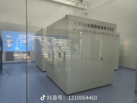
According to sources close to Reuters, China has developed a working prototype of an EUV machine, which is currently undergoing testing. This domestic achievement involved Chinese companies successfully reverse-engineering ASML's EUV lithography scanners and creating a functional version using second-hand components. The new EUV prototype reportedly takes up an entire factory floor, comparable in size to modern High-NA EUV machines from ASML. Chinese companies are said to have obtained parts from older ASML machines on secondary markets. The Chinese government initially set a goal of producing working chips from the prototype by 2028.

Leading this initiative is the Chinese technology giant Huawei, which is working to establish a domestic AI supply chain to bypass foreign tech restrictions. In Guanlan, China, Huawei established a comprehensive facility for manufacturing semiconductors using 7 nm technology for its custom processors. Dissatisfied with SMIC's limited output capacity, Huawei has assumed control of the entire silicon production process, from sourcing materials and chemicals to wafer fabrication equipment and chip design. The company is making an unprecedented effort to develop every component of the AI supply chain domestically, from wafer fabrication equipment to model building, and now EUV scanners for more advanced nodes.

Chinese SMIC Achieves 5 nm Production on N+3 Node Without EUV Tools

Chinese company SMIC has officially achieved volume production of its newest 5 nm-class node called SMIC N+3. This is officially China's most advanced semiconductor node produced without any extreme ultraviolet (EUV) lithography tools, relying on the deep ultraviolet (DUV) to manufacture its silicon. In the latest analysis of the Huawei Kirin 9030 SoC, the TechInsights has confirmed that the chip has officially been manufactured using the new advanced node, bringing Chinese semiconductor independence one step closer to reality. This node is a full generation ahead of the older SMIC N+2, which is 7 nm-class node Huawei has been using to manufacture its Ascend series of AI accelerators and other infrastructure parts.

However, this is not without drawbacks. Since SMIC uses DUV to print silicon designs, the company faces significant challenges in realizing its silicon ambitions. For printing smaller nodes, EUV scanners offer more possibilities due to their much smaller wavelength of 13.5 nm, compared to the smallest DUV immersion scanner wavelength of 193 nm. TechInsights has confirmed that SMIC's N+3 node, despite achieving impressive DUV multi-patterning implementation, encounters significant yield challenges, particularly due to the aggressively scaled metal pitch. As a result, the Huawei Kirin 9030 SoC is likely produced at an operating loss, with a significant portion of dies being discarded or used for downgraded chips.

DNP Achieves 10 nm Line-Pattern Resolution on Nanoimprint Template for Semiconductors

Dai Nippon Printing Co., Ltd. (DNP) today announced the development of a nanoimprint lithography (NIL) template featuring a circuit line width of 10 nanometers (nm: 10-9 meter). The new template enables patterning for logic semiconductors equivalent to the 1.4 nm generation and meets the miniaturization needs of cutting-edge logic semiconductors used in devices such as smartphones, data centers, and NAND flash memory.

Background and Aims
In line with the shift to more sophisticated devices seen in recent years, demands have emerged for even greater miniaturization in cutting-edge semiconductors, leading to advances in Extreme Ultra-Violet (EUV) lithography-based production. EUV lithography, however, requires substantial capital investment, energy consumption, and operating costs in building production lines and the exposure process. This has fed into the pressing need to balance a reduction in manufacturing costs with a lowering in the environmental burden.

Japan Ramps Up Photoresist and MOR Capacity for 2 nm EUV Lithography

As the 2 nm-class nodes are starting to enter volume production, Japanese material suppliers are expanding the capacity of EUV-capable resists and high-purity process chemicals, according to Nikkei. Tokyo Ohka Kogyo (TOK), Adeka, and JSR are building or upgrading fabs for photoresists and metal-oxide resist (MOR) chemistries that improve resolution, line-edge roughness (LER), and etch resistance for extreme ultraviolet patterning. TOK will invest ¥20 billion ($130 million) to add a South Korea photoresist plant (operations targeted for 2030), expanding capacity up to three to four times for packaging and memory customers such as Samsung, TSMC and SK hynix, and a separate ¥12 billion ($78 million) site for high-purity semiconductor chemicals. These chemicals (solvents, developers, surfactants, cleaning agents) are critical for EUV processes where resist sensitivity, contamination control, and outgassing limits directly affect wafer yield and mask lifetime. Adeka's ¥3.2 billion ($20 million) investment will equip its Ibaraki lines for MOR mass production (from ~April 2028), while JSR's MOR facility in South Korea is slated for service by late 2026.

These expansions address bottlenecks unique to EUV lithography technology, such as resist sensitivity vs resolution tradeoffs, defect mitigation and contaminant control. Japan's suppliers already account for the majority of high-end photoresist supply (~91% market share), giving them an edge over competitors that have improved i-line/KrF resist technology but still lag on EUV MOR and process-grade chemical scale-up. MORs contain metal compounds that increase EUV photon absorption and improve pattern transfer: higher absorption reduces dose requirements, and metal-based chemistries can yield better LER and etch durability vs conventional organic resists, a key for sub-2 nm pattern fidelity.

ASML Reports €7.5 Billion Total Net Sales and €2.1 Billion Net Income in Q3 2025

Today, ASML Holding NV (ASML) has published its 2025 third-quarter results.
  • Q3 total net sales of €7.5 billion, gross margin of 51.6%, net income of €2.1 billion
  • Quarterly net bookings in Q3 of €5.4 billion of which €3.6 billion is EUV
  • ASML expects Q4 2025 total net sales between €9.2 billion and €9.8 billion, and a gross margin between 51% and 53%
  • ASML expects a full-year 2025 total net sales increase of around 15% relative to 2024, with a gross margin of around 52%
  • ASML does not expect 2026 total net sales to be below 2025
CEO statement and outlook
"Our third-quarter total net sales of €7.5 billion and gross margin of 51.6% were in line with our guidance, reflecting a good quarter for ASML. On the technology side, we see litho intensity continue to develop positively as EUV adoption gains momentum, including progress on High NA EUV. In line with our plans to support our customers in the 3D integration space, we shipped ASML's first product serving Advanced Packaging, the TWINSCAN XT:260, an i-line scanner offering up to 4x productivity compared to existing solutions. Finally, our partnership with Mistral AI allows us to embed AI across our entire holistic portfolio, in order to increase the performance and productivity of our systems and the yield of our customers' processes."

Texas Instruments Unveils DLP991UUV Digital Micromirror Device for Advanced Packaging

Texas Instruments is enhancing the next generation of digital lithography with the introduction of the DLP991UUV digital micromirror device (DMD), the company's highest resolution direct imaging solution to date. With 8.9 million pixels, sub-micron resolution capabilities and a data rate of 110 gigapixels per second, the device eliminates the need for expensive mask technology while delivering the scalability, cost-effectiveness and precision needed for increasingly complex packaging.

Why it matters
Maskless digital lithography machines - which project light for etching circuit designs on materials without a photomask or high-end stencil - are becoming increasingly popular for the manufacturing of advanced packaging. Advanced packaging combines multiple chips and technologies into a single package, enabling high-computing applications, such as data centers and 5G, to have systems that are smaller, faster, and more power-efficient.

LG Expands xboom Buds Lineup With Buds Plus and Buds Lite for Every Lifestyle

LG Electronics (LG) is expanding the xboom Buds lineup with the introduction of Buds Plus and Buds Lite, building on the success of the original xboom Buds launched in January. Designed to deliver high-quality audio experiences for casual listeners and discerning audiophiles alike, the new models offer immersive sound, extended battery life and ergonomic comfort, ensuring uninterrupted listening wherever life takes you.

Expertly tuned by world-renowned musician will.i.am, the xboom Buds series delivers high-resolution sound quality and rich bass. With this expansion, LG continues to differentiate its audio offerings by providing a diverse range of features and pricing options tailored to different lifestyles - from premium performance to essential everyday use.

TSMC Repurposing Old Fabs to Bring EUV Pellicle Production In-House

TSMC is repurposing its old, wound-down, 8-inch Fab 3 in Hsinchu Science Park to produce extreme ultraviolet pellicles, bringing this production in-house. An EUV pellicle is a thin, highly transparent membrane stretched above a photomask to prevent particles from contacting the mask during EUV exposure. It is designed to withstand intense EUV radiation and thermal stress while minimizing optical absorption and wavefront distortion. Producing pellicles is a way to shorten replacement cycles and exert more control over a component that, in EUV environments, must protect photomasks from particles while coping with extreme exposure conditions. Unlike older DUV processes, EUV systems operate with 400 W light sources and localized heating that can approach 1,000°C at the mask, increasing contamination risks and making pellicle performance more influential to wafer yields.

The economics around pellicles have encouraged divergent approaches. DUV pellicles are relatively inexpensive, at about $720, which has enabled their widespread use in earlier nodes. However, EUV variants have recorded prices near $10,000, which deterred some chipmakers from blanket deployment and may have contributed to documented yield gaps. These pellicles must be replaced every three to four days, too. By internalizing production, TSMC wants to achieve lower per-unit costs and more predictable supply, making pellicle integration viable at scale. That financial case goes hand in hand with materials research: carbon nanotube membranes are the most promising candidate to meet the twin demands of durability and optical transparency. Membranes must resist accelerated degradation from stronger light sources while minimizing absorption that would reduce exposure efficiency. TSMC plans to validate solutions as it ramps N2 and A16 process technologies, where improved pellicle performance could significantly boost yields and preserve its edge on advanced nodes.

Glorious Releases GMBK Membrane Keyboard with MX Keycap Compatibility

Glorious, usually known for its pricey mechanical and Hall effect gaming keyboards, has officially announced the GMBK 75% gaming keyboard. As the name suggests, the GMBK is a 75% gaming keyboard, but instead of mechanical keys, the GMBK uses membrane switches as a way to keep the price down. Unlike most membrane keyboards, though, the GMBK 75% still uses cross stems, making the keyboard compatible with regular MX-compatible keycaps generally used with mechanical keyboards. The GMBK targets the entry-level gaming market, although the pricing is on the higher end of what you might expect from a membrane keyboard, although a membrane keyboard at this price usually doesn't feature MX keycap compatibility or standard plate-mounted stabilizers. It also boasts an IP57 dust- and water-resistance rating, which is unique in the keyboard space.

[Editor's note: Our in-depth review of the Glorious GMMK 3 Pro HE is now live]

The GMBK 75% comes stock with shine-through UV-coated ABS keycaps (no mention of the profile used, but it looks like OEM), which complements the 10-zone RGB backlighting, which is customizable through Glorious Core. Glorious pitches the MX keycap compatibility as a solution for customization, which is usually restricted to expensive mechanical keyboards, but the Glorious GMBK launches at $59.99, which is right around the price of an entry-level mechanical keyboard, especially when you're willing to forego wireless connectivity. The Glorious GMBK is also wired-only, but it still utilizes a detachable USB Type-C cable, which, along with the keycap compatibility, is a boon for repairability. Glorious doesn't make mention of NKRO, but the spec sheet confirms that 1 kHz polling is present, which should be responsive enough for most gamers. In keeping with the "budget" target market, the GMBK is entirely made of plastic and comes in at 540 g weight, unlike many mechanical boards, which exceed the 1 kg mark. Glorious has still seen fit to include a knob on the GMBK, which is a somewhat premium touch, given the price.


Rapidus Achieves Significant Milestone with Prototyping of Leading-Edge 2nm GAA Transistors

Rapidus Corporation, a manufacturer of advanced logic semiconductors, today announced that prototyping has started for its 2 nm gate-all-around (GAA) transistor structure at Rapidus Innovative Integration for Manufacturing (IIM-1) foundry. The prototype wafers also started to obtain their electrical characteristics. Rapidus new IIM-1 foundry represents a significant advancement over the traditional foundry model. The company is re-imagining how semiconductor factories should think, learn, adapt and optimize processes in real time through cutting-edge methods and technology including:

Fully single-wafer front-end processing: In a single-wafer process, adjustments can be made to a single wafer, inspected and if successful, applied to all subsequent wafers. Single wafer captures more data, enabling AI models to be trained to improve wafer production and increase yields. Rapidus is one of the first companies that will commercialize fully single-wafer processing, which is central to its Rapid and Unified Manufacturing Service (RUMs).

Yeston Reveals Radeon RX 9060 XT Game Ace 16 GB Model

Roughly a month ago, Yeston introduced its new generation Game Ace design along with a mysterious no. 207 mascot. The Chinese manufacturer is best known for creating bright and sparkly graphics cards, but a couple of darker products have emerged from their HQ. Their latest offering—finished in varying tones of pink, purple and black—was debuted with GeForce RTX 50-series hardware. At the start of this week, the 2025 Game Ace lineup welcomed a new member. Yeston's social media accounts introduced a custom Radeon RX 9060 XT 16 GB model: "the black and purple cyberpunk RX 9060 XT Game Ace launched today. Would he be your choice?" In a reply to a follower's question, a company rep confirmed that the better known Sakura and Sakura Atlantis backplate/shroud designs are currently reserved for higher-end Radeon RX 9070 XT and non-XT options (within the RDNA 4 family). Game Ace will probably not escape the confines of Navi 44 (XT) hardware.

Unsurprisingly, the Yeston Radeon RX 9060 XT 16 GB Game Ace SKU exhibits only minor visual differences, when compared to its "Blackwell" GPU-based relatives. We are looking at a fairly typical triple-fan + three 6 mm heat pipes cooling solution. A single 8-pin power connector is visible in some of Yeston's promotional renders. According to ITHome's inspection of specifications: "the boost frequency and game frequency under standard mode (STD) are 3230 MHz and 2620 MHz respectively, and the VAR mode further overclocks to 3230 MHz and 2780 MHz." Despite claiming that their freshly unveiled Game Ace model has reached launch status, the AIB likely has to conform with official AMD decree. Team Red's board partners will be releasing Radeon RX 9060 XT cards on June 5.

China Develops Domestic EUV Tool, ASML Monopoly in Trouble

China's domestic extreme ultraviolet (EUV) lithography development is far from a distant dream. The newest system, now undergoing testing at Huawei's Dongguan facility, leverages laser-induced discharge plasma (LDP) technology, representing a potentially disruptive approach to EUV light generation. The system is scheduled for trial production in Q3 2025, with mass manufacturing targeted for 2026, potentially positioning China to break ASML's technical monopoly in advanced lithography. The LDP approach employed in the Chinese system generates 13.5 nm EUV radiation by vaporizing tin between electrodes and converting it to plasma via high-voltage discharge, where electron-ion collisions produce the required wavelength. This methodology offers several technical advantages over ASML's laser-produced plasma (LPP) technique, including simplified architecture, reduced footprint, improved energy efficiency, and potentially lower production costs.

The LPP method relies on high-energy lasers and complex FPGA-based real-time control electronics to achieve the same result. While ASML has refined its LPP-based systems over decades, the inherent efficiency advantages of the LDP approach could accelerate China's catch-up timeline in this critical semiconductor manufacturing technology. When the US imposed sanctions on EUV shipments to Chinese companies, the Chinese semiconductor development was basically limited as standard deep ultraviolet (DUV) wave lithography systems utilize 248 nm (KrF) and 193 nm (ArF) wavelengths for semiconductor patterning, with 193 nm immersion technology representing the most advanced pre-EUV production technique. These longer wavelengths contrast with EUV's 13.5 nm radiation, requiring multiple patterning techniques to achieve advanced nodes.
Return to Keyword Browsing
Nov 11th, 2026 03:59 CST change timezone

New Forum Posts

Popular Reviews

TPU on YouTube

Controversial News Posts