Monday, February 9th 2026
Imec Inaugurates NanoIC Pilot Line, Accelerating Innovation in Sub-2nm Systems-On-Chip
Imec - a world-leading R&D center in advanced semiconductor technologies - today inaugurated a 2,000 m² cleanroom expansion at its Leuven headquarters, marking a pivotal milestone in the deployment of Europe's NanoIC pilot line. The event was attended by European EVP Henna Virkkunen, Belgian Prime Minister Bart De Wever, Flemish Minister-President Matthias Diependaele, and ASML CEO Christophe Fouquet, alongside representatives from the European high-tech ecosystem - including industry and startups - the NanoIC pilot line consortium, and policymakers from the EU, Belgium, and Flanders. With a capacity of over 12,000 m², imec's cleanroom plays a crucial role in the European Chips Act's ambitions to position Europe at the forefront of next-generation semiconductor innovation and manufacturing; a strategy that will be instrumental in reinforcing the continent's industrial fabric in the AI era, while safeguarding a climate of sustained economic growth, security, and prosperity for decades to come.
"Since announcing in May 2024 that imec would host the NanoIC pilot line, we've moved at full speed - accelerating tool acquisition and launching a comprehensive recruitment program. Today, that effort culminates in the inauguration of a 2,000 m² cleanroom extension at the imec premises. It will house a best-in-class toolset, including ASML's next-generation High NA EUV scanner that is scheduled to arrive mid-March," said Luc Van den hove, CEO of imec.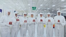
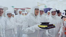
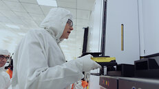 "Imec researchers are working here side by side with IDMs, foundries, equipment and materials suppliers, system companies, start-ups, universities, and fellow European RTOs. Together, we have embarked on an ambitious journey to push semiconductor technologies beyond the 2 nm node. By providing access to cutting-edge semiconductor technologies, the NanoIC pilot line will play a crucial role in strengthening Europe's industrial fabric in the AI era, and ensuring a climate of economic growth, security, and prosperity for decades to come," he added.
Strategic Importance and Future Outlook
And the momentum continues. With strong backing from the European, Belgian, and Flemish governments - and a robust network of industry partners - imec will soon begin construction of a whole new 4,000 m² cleanroom at its Leuven campus, another key asset to bring Europe's NanoIC initiative to full cruising speed. Over the next five years, the NanoIC pilot line will integrate more than a hundred new tools, distributed across imec and partner sites at CEA-Leti (France), Fraunhofer (Germany), VTT (Finland), CSSNT-UPB (Romania), and Tyndall National Institute (Ireland).
"We don't have the luxury of being the biggest or the strongest, but we do have the choice to be the best," explains Matthias Diependaele, Flemish Minister-President. "Imec brings together talent, knowledge, and international collaboration. With the NanoIC pilot line, Europe is making that choice a reality: for technological excellence and strategic independence. The fact that imec is hosting this pilot line underscores the exceptional strengths that Flanders has developed in research and innovation. Here, we are demonstrating how a world-class region can shape the chip technology of tomorrow."
A Step Forward for European Semiconductor Leadership
Christophe Fouquet, President and CEO of ASML: "Today we are making a step forward in strengthening the chip technology ecosystem in Europe to serve our customers, the world's chipmakers. Through our 40 years partnership at imec, together we have been driving faster innovation, fostering stronger collaboration, and supporting the development of regional talent, all of which are needed to support the advancement of the worldwide chip industry and AI. We are today inaugurating the NanoIC pilot line, that includes ASML's High NA EUV system and which is the best example of what we can do when worldwide leaders in technology partner to bring together their latest technology and talent. Thanks to the strong support of EU President Von der Leyen and the European Chips Act, we are all very proud and thankful that this is happening at the heart of Europe and will allow Europe to play an even more critical role in the global semiconductor ecosystem"
Source:
Imec
"Since announcing in May 2024 that imec would host the NanoIC pilot line, we've moved at full speed - accelerating tool acquisition and launching a comprehensive recruitment program. Today, that effort culminates in the inauguration of a 2,000 m² cleanroom extension at the imec premises. It will house a best-in-class toolset, including ASML's next-generation High NA EUV scanner that is scheduled to arrive mid-March," said Luc Van den hove, CEO of imec.


Strategic Importance and Future Outlook
And the momentum continues. With strong backing from the European, Belgian, and Flemish governments - and a robust network of industry partners - imec will soon begin construction of a whole new 4,000 m² cleanroom at its Leuven campus, another key asset to bring Europe's NanoIC initiative to full cruising speed. Over the next five years, the NanoIC pilot line will integrate more than a hundred new tools, distributed across imec and partner sites at CEA-Leti (France), Fraunhofer (Germany), VTT (Finland), CSSNT-UPB (Romania), and Tyndall National Institute (Ireland).
"We don't have the luxury of being the biggest or the strongest, but we do have the choice to be the best," explains Matthias Diependaele, Flemish Minister-President. "Imec brings together talent, knowledge, and international collaboration. With the NanoIC pilot line, Europe is making that choice a reality: for technological excellence and strategic independence. The fact that imec is hosting this pilot line underscores the exceptional strengths that Flanders has developed in research and innovation. Here, we are demonstrating how a world-class region can shape the chip technology of tomorrow."
A Step Forward for European Semiconductor Leadership
Christophe Fouquet, President and CEO of ASML: "Today we are making a step forward in strengthening the chip technology ecosystem in Europe to serve our customers, the world's chipmakers. Through our 40 years partnership at imec, together we have been driving faster innovation, fostering stronger collaboration, and supporting the development of regional talent, all of which are needed to support the advancement of the worldwide chip industry and AI. We are today inaugurating the NanoIC pilot line, that includes ASML's High NA EUV system and which is the best example of what we can do when worldwide leaders in technology partner to bring together their latest technology and talent. Thanks to the strong support of EU President Von der Leyen and the European Chips Act, we are all very proud and thankful that this is happening at the heart of Europe and will allow Europe to play an even more critical role in the global semiconductor ecosystem"
7 Comments on Imec Inaugurates NanoIC Pilot Line, Accelerating Innovation in Sub-2nm Systems-On-Chip
intel would have gotten 9.9billion in subsidies for a 30 billion plant.
They pioneered lots, and with this expansion i hope they will invent a lot more things that will make transistors smaller and more efficient.