Monday, February 23rd 2026

ASML Boosts EUV Power to 1,000W for Better Yields and Lower Chip Costs
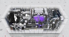
ASML says it has boosted the light source power in its EUV lithography systems to 1,000 watts, up from roughly 600 W today. According to a Reuters report, the company claims the increase could enable up to 50% more chip output by the end of the decade. More source power translates directly into higher throughput. ASML says customers could process around 330 wafers per hour by 2030, compared to about 220 wafers per hour today, lowering the cost per chip. EUV light at a 13.5 nm wavelength is generated by firing a CO₂ laser at microscopic droplets of molten tin, creating plasma that emits EUV radiation. The light is then collected and directed through precision optics supplied by Carl Zeiss AG. To reach 1,000 W, ASML doubled the droplet rate to roughly 100,000 per second and shifted to a two-pulse laser shaping approach instead of a single pulse. The company says there is a path toward 1,500 W and potentially even 2,000 W over time.
ASML is the only supplier of commercial EUV scanners, used by major chipmakers including TSMC, SK Hynix, and Intel. The tools are considered critical to advanced node production and have been subject to export restrictions to China. The move is aimed at maintaining ASML's lead as U.S. companies, such as Pat Gelsinger's xLight EUV startup and Chinese efforts to develop competing lithography systems continue to ramp. Chinese companies have reportedly been sourcing parts from older ASML machines through secondary markets. Huawei is leading the charge, working to build a homegrown AI supply chain as a way around foreign tech restrictions. The company set up a large semiconductor manufacturing facility in Guanlan focused on 7 nm chips for its own processors. The Chinese government had initially aimed to have a working prototype from this effort by 2028.
Source:
Reuters
ASML is the only supplier of commercial EUV scanners, used by major chipmakers including TSMC, SK Hynix, and Intel. The tools are considered critical to advanced node production and have been subject to export restrictions to China. The move is aimed at maintaining ASML's lead as U.S. companies, such as Pat Gelsinger's xLight EUV startup and Chinese efforts to develop competing lithography systems continue to ramp. Chinese companies have reportedly been sourcing parts from older ASML machines through secondary markets. Huawei is leading the charge, working to build a homegrown AI supply chain as a way around foreign tech restrictions. The company set up a large semiconductor manufacturing facility in Guanlan focused on 7 nm chips for its own processors. The Chinese government had initially aimed to have a working prototype from this effort by 2028.


9 Comments on ASML Boosts EUV Power to 1,000W for Better Yields and Lower Chip Costs
Back when I used to weld, I output in excess of 2kW of power. While most of it was IR, there was so much UV, anything that was damaged by UV would be toast at the end of a shift. Ozone was so plentiful, that prob did the most damage....feet away
So, what is so special about a 400W jump? While I have never been to a wafer fab, I did go to a shop that built the components that went into the machines...think exotic metals for high purity vacuum developement
And if I got it right from the video, I think I heard them say the laser to blast the tin was 20kW. And also, it is all about the lambda at a specific, increasing power.
I was very suprised by the addition of O² to keep the mirror clean.