Tuesday, December 9th 2025
DNP Achieves 10 nm Line-Pattern Resolution on Nanoimprint Template for Semiconductors
Dai Nippon Printing Co., Ltd. (DNP) today announced the development of a nanoimprint lithography (NIL) template featuring a circuit line width of 10 nanometers (nm: 10-9 meter). The new template enables patterning for logic semiconductors equivalent to the 1.4 nm generation and meets the miniaturization needs of cutting-edge logic semiconductors used in devices such as smartphones, data centers, and NAND flash memory.
Background and Aims
In line with the shift to more sophisticated devices seen in recent years, demands have emerged for even greater miniaturization in cutting-edge semiconductors, leading to advances in Extreme Ultra-Violet (EUV) lithography-based production. EUV lithography, however, requires substantial capital investment, energy consumption, and operating costs in building production lines and the exposure process. This has fed into the pressing need to balance a reduction in manufacturing costs with a lowering in the environmental burden.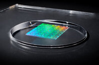
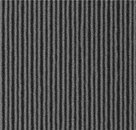 Since 2003, DNP has been developing NIL templates, used to press circuit patterns directly into substrate materials, allowing manufacturers to reduce energy consumption in the exposure process. Over the following two decades, DNP has successfully accumulated extensive know-how in high-precision patterning.
In this latest development, DNP has developed a NIL template with a 10 nm line pattern. It can replace a portion of the EUV lithography process, facilitating the manufacture of cutting-edge logic semiconductors for clients that do not have EUV lithography production processing. By supplying the new template, DNP will expand the options available to clients involving semiconductor manufacturing processes, helping to reduce both manufacturing costs and the environmental burden.
Key Features
Anticipating semiconductor miniaturization needs, DNP is engaging in a deeper dialogue with semiconductor manufacturer clients. We have begun evaluation work for NIL templates, and aim to start mass production in 2027. DNP will advance the further development of NIL templates and enhance production capacity to meet growing demand, targeting increased NIL sales of 4 billion yen in FY 2030.
The new 10 nm NIL template will be exhibited at the DNP booth, situated at East Hall 6, E5936 at SEMICON Japan 2025, to be held December 17-19 at Tokyo Big Sight.
Source:
Dai Nippon Printing
Background and Aims
In line with the shift to more sophisticated devices seen in recent years, demands have emerged for even greater miniaturization in cutting-edge semiconductors, leading to advances in Extreme Ultra-Violet (EUV) lithography-based production. EUV lithography, however, requires substantial capital investment, energy consumption, and operating costs in building production lines and the exposure process. This has fed into the pressing need to balance a reduction in manufacturing costs with a lowering in the environmental burden.


In this latest development, DNP has developed a NIL template with a 10 nm line pattern. It can replace a portion of the EUV lithography process, facilitating the manufacture of cutting-edge logic semiconductors for clients that do not have EUV lithography production processing. By supplying the new template, DNP will expand the options available to clients involving semiconductor manufacturing processes, helping to reduce both manufacturing costs and the environmental burden.
Key Features
- DNP has successfully achieved further miniaturization of NIL templates by leveraging Self-Aligned Double Patterning (SADP), which doubles pattern density through film deposition and etching a pattern formed by an electron beam mask writer.
- In addition to the photomask manufacturing technology and know-how cultivated by DNP, wafer manufacturing process technology has also been applied to develop the new NIL template with a circuit line width of 10 nm.
- The new NIL template answers the need for finer circuit line widths in advanced logic semiconductors, which are expected to continue expanding in the future.
- The technology also reduces power consumption in the exposure process of cutting-edge semiconductor manufacturing. Driven by an energy-saving processing technology for ultra-fine semiconductors using NIL, it is now possible to reduce power consumption to approximately one-tenth of currently available exposure processes, such as Argon Fluoride (ArF) immersion and EUV.
Anticipating semiconductor miniaturization needs, DNP is engaging in a deeper dialogue with semiconductor manufacturer clients. We have begun evaluation work for NIL templates, and aim to start mass production in 2027. DNP will advance the further development of NIL templates and enhance production capacity to meet growing demand, targeting increased NIL sales of 4 billion yen in FY 2030.
The new 10 nm NIL template will be exhibited at the DNP booth, situated at East Hall 6, E5936 at SEMICON Japan 2025, to be held December 17-19 at Tokyo Big Sight.
4 Comments on DNP Achieves 10 nm Line-Pattern Resolution on Nanoimprint Template for Semiconductors
"
The energy required to produce semiconductors is enormous—semiconductor manufacturing is one of the most energy-intensive industrial processes on Earth. Here's a breakdown with concrete numbers (mostly based on modern 3nm–5nm class nodes like TSMC's, which are the current state-of-the-art in 2024–2025):
Energy per Wafer (300 mm)
- A single leading-edge 300 mm wafer (containing hundreds to thousands of chips depending on die size) requires 15–25 MWh of electricity from start to finish.
"In addition:
"
TL;DR: Making one cutting-edge smartphone chip consumes as much electricity as driving a Tesla Model 3 more than 5,000–10,000 km. A single high-end AI GPU can embody as much energy as an average European uses in an entire year. Semiconductors are incredibly energy-expensive to manufacture.
"
Seriously? Dang...who knew?!?!?!? I guess a 1/10 energy reduction is a big deal when we're talking MW scale. Makes me really thankful for what I currently have. And dang...makes me think all these NVIDIA chips going into Ai centers...it's not just the energy needed for the Data center but just the manufacturing...
The scale in semiconductor manufacturing is just amazing, enough to look at fab pictures and compare them to car manufacturing.. if you go into details about energy, raw materials, and so on, it becomes a spider web.
It takes exponentially more energy to produce light with shorter wavelengths.
In fact, EUV light is produced by vaporizing tin droplets with an extremely power laser, turning it into plasma 40 times hotter than the surface of the sun.
Light with shorter wavelengths also need to be more focused. Reflecting EUV light (we can barely generate enough energy to produce) 10-12 times, with each mirror absorbing 30% of the light, and you end up with less than 1% of EUV light hits the wafer.
Mistake number 2 : using Grok, of all LLMs, to do anything at allThis is entirely false :
english.cw.com.tw/article/article.action?id=3786
ASML being the very company the manufactures the machines engraving silicon wafers for basically all major foundries around the world
Do yourself a service and never rely on LLMs to research anything ever again.