News Posts matching #iGPU

Return to Keyword Browsing

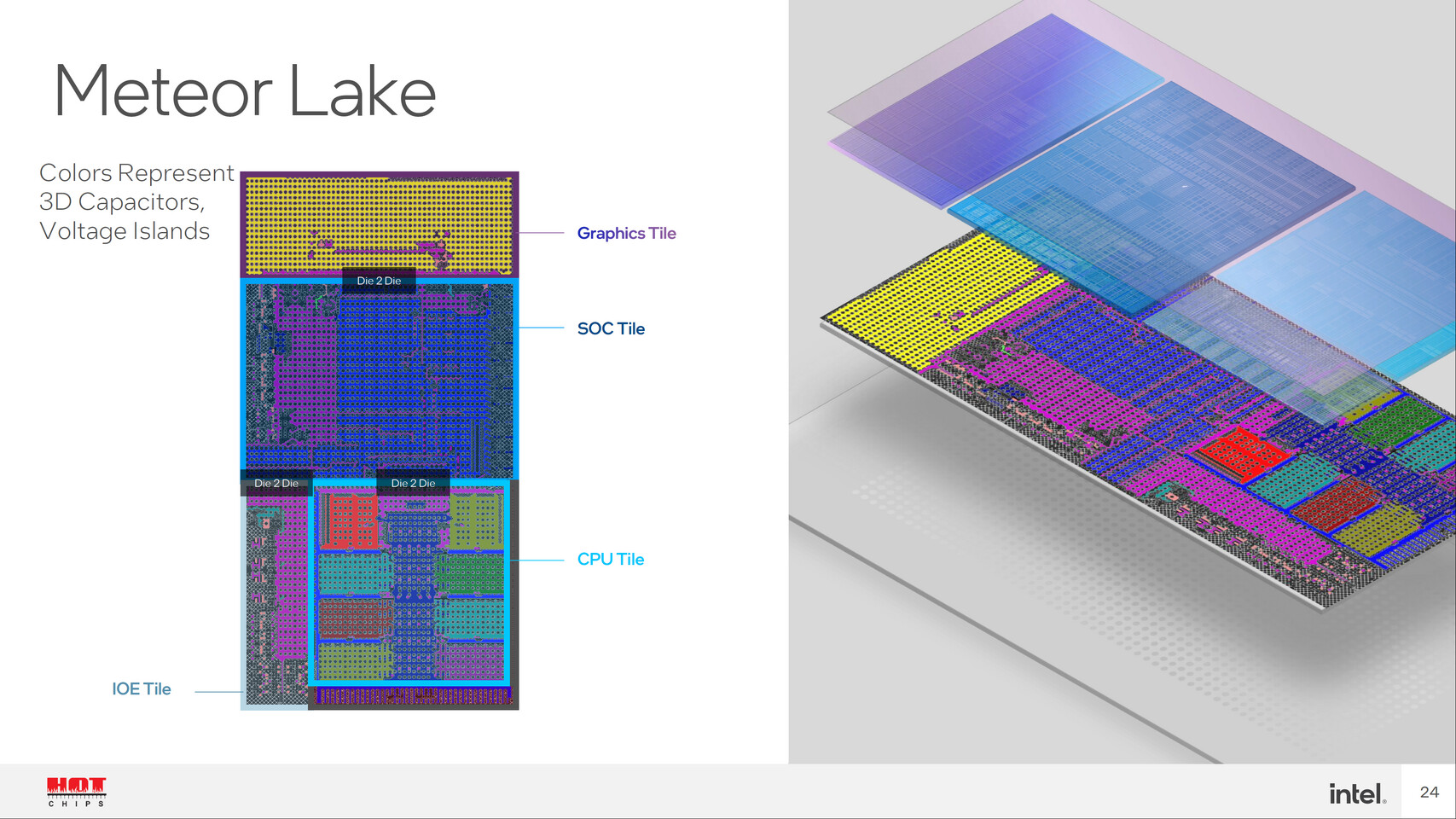
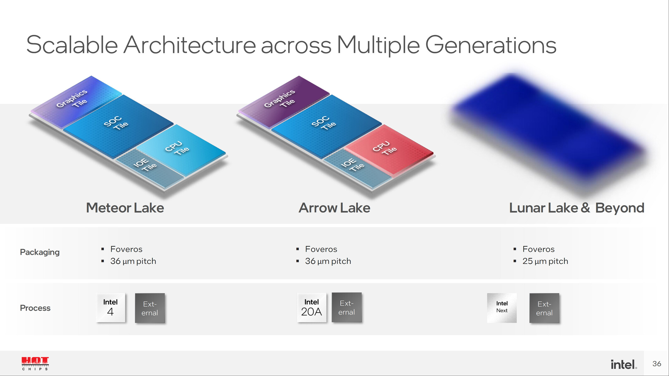
Intel Defers 3 nm Wafer Orders with TSMC, Pushes "Arrow Lake" Rollout to 2025?

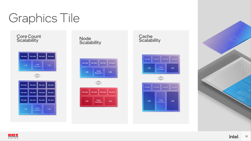
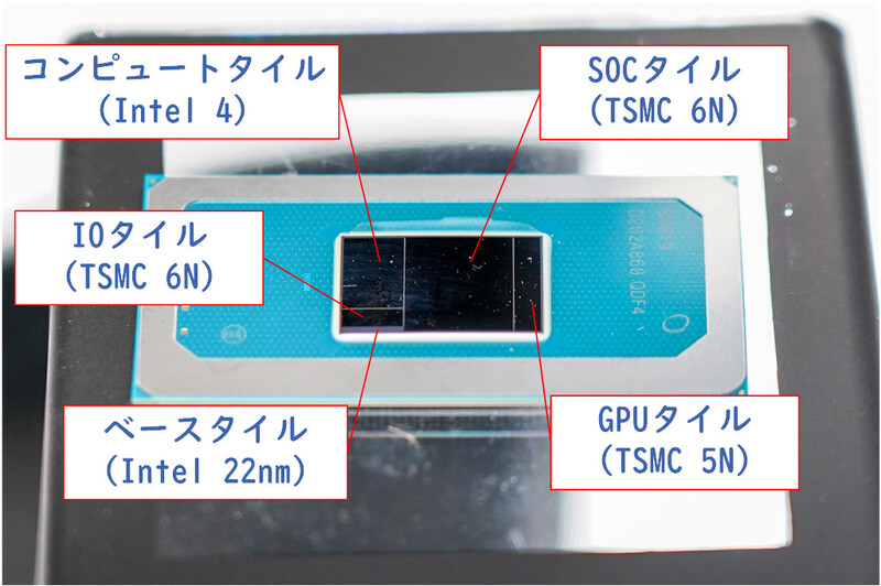
Intel has reportedly deferred its orders for 3 nm wafers with TSMC, sources in PC makers tell Taiwan-based industry observer DigiTimes. Built on the TSMC N3 node, the wafers were supposed to power the Graphics tiles (containing the iGPU), of the upcoming "Arrow Lake" processors, which were originally on course for a 2024 release. The DigiTimes report detailing this development says that Intel's 3 nm wafer orders have been deferred to Q4-2024, which would realistically mean a 2025 launch for whatever product was designed to use 3 nm tiles. Advance orders for next-gen wafers by high-volume clients such as Intel, are usually placed several quarters in advance, so the foundry could suitably scale up its capacity.

AMD RDNA4 Architecture to Build on Features Relevant to Gaming Performance, Doesn't Want to be Baited into an AI Feature Competition with NVIDIA

AMD's next-generation RDNA4 graphics architecture will retain a design-focus on gaming performance, without being drawn into an AI feature-set competition with rival NVIDIA. David Wang, SVP Radeon Technologies Group; and Rick Bergman, EVP of Computing and Graphics Business at AMD; gave an interview to Japanese tech publication 4Gamers, in which they dropped the first hints on the direction which the company's next-generation graphics architecture will take.

While acknowledging NVIDIA's movement in the GPU-accelerated AI space, AMD said that it didn't believe that image processing and performance-upscaling is the best use of the AI-compute resources of the GPU, and that the client segment still hasn't found extensive use of GPU-accelerated AI (or for that matter, even CPU-based AI acceleration). AMD's own image processing tech, FSR, doesn't leverage AI acceleration. Wang said that with the company introducing AI acceleration hardware with its RDNA3 architecture, he hopes that AI is leveraged in improving gameplay—such as procedural world generation, NPCs, bot AI, etc; to add the next level of complexity; rather than spending the hardware resources on image-processing.

Intel Meteor Lake to Feature 50% Increase in Efficiency, 2X Faster iGPU

Intel's upcoming Meteor Lake processor family is supposedly looking good with the new performance/efficiency targets. According to the @OneRaichu Twitter account, we have a potential performance estimate for the upcoming SKUs. As the latest information notes, Intel's 14th-generation Meteor Lake will feature around a 50% increase in efficiency compared to the 13th-generation Raptor Lake designs. This means that the processor can use half the power at the same performance target at Raptor Lake, increasing efficiency. Of course, the design also offers some performance improvements besides efficiency that are significant and are yet to be shown. The new Redwood Cove P-cores will be combined with the new Crestmont E-cores for maximum performance inside U/P/H configurations with 15-45 Watt power envelopes.

For integrated graphics, the source notes that Meteor Lake offers twice the performance of iGPU found on Raptor Lake designs. Supposedly, Meteor Lake will feature 128 EUs running 2.0+GHz compared to 96 EUs found inside Raptor Lake. The iGPU architecture will switch from Intel Iris to Xe-LPG 'Xe-MTL' family on the 14th gen models, confirming a giant leap in performance that iGPU is supposed to experience. Using the tile-based design, Intel combines the Intel 4 process for the CPU tile and the TSMC 5 nm process for the GPU tile. Intel handles final packaging for additional tuning, and you can see the separation below.

Intel Talks "Battlemage" Xe2-LPG and Xe2-HPG Graphics Architectures

Intel in an interview with Hardwareluxx shed more light on its second generation Xe graphics architecture, codenamed "Battlemage." There will be two key variants of "Battlemage,"—Xe2-LPG and Xe2-HPG. The Xe2-LPG (low-power graphics) architecture is a slimmed-down derivative of "Battlemage" that's optimized for low-power. It is meant for iGPUs (integrated graphics), particularly upcoming "disaggregated" Intel Core processors in which the iGPU exists on Graphics Tiles (chiplets). The iGPU powering the upcoming Core "Meteor Lake" processor is rumored to meet the full DirectX 12 Ultimate feature-set (something Xe-LP doesn't), and so it's likely that Xe2-LPG is getting its first outing with that processor. The Xe2-HPG (high performance graphics) architecture is designed squarely for discrete GPUs—either desktop graphics cards, or mobile discrete GPUs hardwired into laptops.

In the interview, Intel talked about how its first-generation Xe graphics IP had at least four separate product verticals based on the scalability of the product, and the specific application (Xe-LP for iGPUs and tiny dGPUs, Xe-HPG for client- and pro-vis discrete GPUs, Xe-HPC for scalar compute processors, and Xe-HP for data-center graphics). The company eventually axed Xe-HP as it felt the Xe-HPG and Xe-HPC architectures adequately addressed this segment. With AXG (accelerated compute group) being split up between the CCG (client computing group) and DCG (data-center group); Xe2-LPG and Xe2-HPG will be developed primarily under CCG, with a client and pro-visualization focus; while Xe-HPC will be developed as a scalar-compute architecture by DCG, which effectively leaves the Intel Arc Graphics team with just two verticals—to deliver a feature-rich iGPU for its next-generation Core processors, and a performance discrete GPU lineup so it can eat away market-share from NVIDIA and AMD—hopefully with better time-to-market.

Intel Core "Meteor Lake" On Course for 2H-2023 Launch

Intel in its Q4-2022 Financial release call reiterated that its Core "Meteor Lake" processor remains on course for a 2H-2023 launch. The company slide does not mention the client form-factor the architecture targets, and there are still rumors of a "Raptor Lake Refresh" desktop processor lineup for 2H, which would mean that "Meteor Lake" will debut as a high-performance mobile processor architecture attempting to dominate the 7 W, 15 W, 28 W, and 35 W device market-segments, with its 6P+16E CPU that introduce IPC increases on both the P-cores and E-cores; and a powerful new iGPU. The slide also mentions that its succeeding "Lunar Lake" architecture is on course for 2024.

"Meteor Lake" is Intel's first chiplet-based MCM processor, in which the key components of the processor are built on various silicon fabrication nodes, based on their need for such a cutting-edge node; such that the cost-optimization upholds the economic aspect of Moore's Law. The compute tile, the die that has the CPU cores, features a 6P+16E setup, with six "Redwood Cove" P-cores, and sixteen "Crestmont" E-cores. At this point it's not known if "Crestmont" cores are arranged in clusters of 4 cores, each. The graphics tile features a powerful iGPU based on the newer Xe-LPG graphics architecture that meets full DirectX 12 Ultimate feature-set. The processor's I/O is expected to support even faster DDR5/LPDDR5 memory speeds, and feature PCIe Gen 5.

Intel Arc GPU Graphics Drivers 101.4090 Beta Released

Intel Graphics today released the latest version of its Arc GPU Graphics Drivers. Version 101.4090 beta comes with launch-day optimization for "Forspoken." The company also fixed a couple of issues with this release. For Arc "Alchemist" discrete GPUs, an application freeze issue with "A Plague Tale: Requiem" has been fixed. Box corruptions noticed in "Need for Speed: Unbound," have also been fixed. For Intel Core processors with Xe LP-based iGPUs, a screenspace corruption issue with NFS: Unbound has been fixed; besides an intermittent application crash with Total War: Warhammer III in DirectX 11 mode, and color corruption in Battlefield: 2042. Grab the drivers from the link below.

DOWNLOAD: Intel Arc GPU Graphics Drivers 101.4090 beta

AMD Announces Ryzen 7040 "Phoenix Point" Mobile Processor: 4nm, Zen 4, RDNA3, XDNA

AMD today launched two distinct kinds of mobile processors, the Ryzen 7045 "Dragon Range" serves the 45 W H- and HX-segments of performance and enthusiast notebooks with CPU core counts of up to 16-core/32-thread; while the U-segment, P-segment, and a portion of the H-segment (ranges of 15 W, 28 W, and 35 W), will be led by the Ryzen 7040 "Phoenix Point." Unlike the "Dragon Range" MCM, "Phoenix Point" is a monolithic silicon built entirely on the TSMC 4 nm EUV foundry node, and introduces a wealth of process-level and system-level power-management features.

AMD "Phoenix Point" combines an 8-core/16-thread CPU based on the "Zen 4" microarchitecture, with a powerful iGPU based on the latest RDNA3 graphics architecture, and a feature-packed AI acceleration engine based on the XDNA architecture AMD built after the Xilinx acquisition. The CPU component is a fully-fledged "Zen 4" CCX, with 8 CPU cores featuring 1 MB of dedicated L2 cache per-core, and sharing a large 32 MB L3 cache. This is an increase from the previous generation "Rembrandt" and "Cezanne" dies that had a reduced 16 MB L3 shared among the eight "Zen 3" or "Zen 3+" CPU cores.

TechPowerUp GPU-Z v2.52.0 Released

TechPowerUp today released the latest version of TechPowerUp GPU-Z, the popular PC graphics information, monitoring, and diagnostics utility. Version 2.52.0 adds support for AMD Radeon RX 7900 XTX, RX 7900 XT, RX 6300 OEM; NVIDIA GeForce RTX 4070 Ti, and a few rare "Ampere" based GPUs in circulation these days, including the RTX 3080 Ti 20 GB, RTX 3070 Ti based on GA102 silicon, RTX 3050 based on GA107, and the PCIe AIC version of the A800 80 GB accelerator. Detection is improved for the Xe LP-based iGPU of Intel Core "Raptor Lake" processors. NVIDIA GPUs with ECC memory now have ECC status reported in the Advanced panel. On GPUs where the boost frequency can't be read, the base frequency will be used to calculate fillrates. Clock speed detection for Intel Arc "Alchemist" GPUs has been improved. Vendor detection has been added for several new graphics card brands such as Corsair (gaming notebooks), Maxsun, and Wingtech.

DOWNLOAD: TechPowerUp GPU-Z v2.52.0

Intel Confirms LGA1851 is its Next Desktop CPU Socket

Intel as part of its development process with industry partners and OEMs, allegedly released technical documents in a bare URL that's worded to confirm that its next desktop processor socket will in fact be the LGA1851. We've had some idea since June 2021 that LGA1851 will succeed LGA1700, but this can be taken as a confirmation. Although with a higher pin-count, the LGA1851 package will be physically of an identical size to LGA1700, with mostly identical socket mechanism, so the new socket could maintain cooler compatibility with its predecessor. The additional 151 pins come from shrinking the "courtyard" (the region of the land grid in the center that lacks pins and instead has some electrical ancillaries).

The new Socket LGA1851 platform is expected to power Intel's "Meteor Lake-S" and "Arrow Lake-S" microarchitectures. Whether "Meteor Lake-S" gets the 14th Gen Core branding is a whole different question. Leaked benchmarks suggest that 2023 will be a rather slow year from Intel in the area of desktop processors, and that toward Q3-2023, the company will release the so-called "Raptor Lake Refresh" processors. These chips are likely built on the same LGA1700 package, and as we've seen from "Coffee Lake Refresh," could warrant a new generational branding to 14th Gen Core (as CFL Refresh formed the 9th Gen Core). Intel could increase clock-speeds, E-core counts, and other process/packaging-level innovations to segment these chips apart from existing 13th Gen Core "Raptor Lake." LGA1851 processors like "Meteor Lake" could debut chiplets for Intel, as these have their CPU cores, iGPU, memory-controllers, and uncore components, spread apart on chiplets built on various foundry nodes.

Intel's Next-Gen Desktop Platform Intros Socket LGA1851, "Meteor Lake-S" to Feature 6P+16E Core Counts

Keeping up with the cadence of two generations of desktop processors per socket, Intel will turn the page of the current LGA1700, with the introduction of the new Socket LGA1851. The processor package will likely have the same dimensions as LGA1700, and the two sockets may share cooler compatibility. The first processor microarchitecture to debut on LGA1851 will be the 14th Gen Core "Meteor Lake-S." These chips will feature a generationally lower CPU core-count compared to "Raptor Lake," but significantly bump the IPC on both the P-cores and E-cores.

"Raptor Lake" is Intel's final monolithic silicon client processor before the company pivots to chiplets built on various foundry nodes, as part of its IDM 2.0 strategy. The client-desktop version of "Meteor Lake," dubbed "Meteor Lake-S," will have a maximum CPU core configuration of 6P+16E (that's 6 performance cores with 16 efficiency cores). The chip has 6 "Redwood Cove" P-cores, and 16 "Crestmont" E-cores. Both of these are expected to receive IPC uplifts, such that the processor will end up faster (and hopefully more efficient) than the top "Raptor Lake-S" part. Particularly, it should be able to overcome the deficit of 2 P-cores.

AMD Ryzen 7 7700 (non-X) Surfaces; Possibly OEM-only

AMD is preparing to expand its Ryzen 7000-series "Zen 4" desktop processor series with new SKUs, one of which is the Ryzen 7 7700 (non-X). Given past trends with non-X SKUs for the Ryzen 5000-series, the 7700 is very likely an OEM-only SKU to be featured in pre-built desktops. The inclusion of an iGPU with the Ryzen 7000-series changes things dramatically for AMD, as it makes these processors suitable for even home- and commercial desktops that lack discrete graphics. The Ryzen 7 7700 has the same 8-core/16-thread configuration as the Ryzen 7 7700X, but likely lower clock-speeds, due to the lower power-limits. The chip has a TDP of 65 W, compared to the 105 W of the 7700X; which means its package power tracking (PPT) power limit will be closer to 90 W, than the 140 W of the 7700X. This will also significantly lower the cooling requirements for the processor, and OEMs could use cost-effective air coolers. The exact clock-speeds, though, remain under the wraps.

Intel Core i3 N300 is a Core Processor with Just E-cores That Somehow Isn't an Atom or Pentium Silver

The upcoming Intel Core i3-N300 is an upcoming entry-level mobile processor that only has "Gracemont" E-cores, no P-cores, and yet somehow isn't branded under Atom or Pentium Silver. This isn't just because Intel retired the entry-level brands in favor of a generic "Intel Inside" brand to be used on entry-level notebooks; but very likely because of the way these chips are architected.

The i3-N300 and i3-N305 were spotted in separate Geekbench submissions discovered by Benchleaks. The chip is identified as having 8 cores and 8 logical processors (threads), but its cache is identified as being 4x 64 KB L1I, with 4x 32 KB L1D, 1x 2 MB L2, and 1x 6 MB L3. It's possible that the chip's design is very similar to a conventional "Alder Lake" processor—with a centralized L3 cache and client interconnect fabric, an uncore, and an iGPU; but with no P-cores, just the two "Gracemont" E-core clusters, each with 2 MB of L2 cache shared among 4 cores.

TSMC (Not Intel) Makes the Vast Majority of Logic Tiles on Intel "Meteor Lake" MCM

Intel's next-generation "Meteor Lake" processor is the first mass-production client processor to embody the company's IDM 2.0 manufacturing strategy—one of building processors with multiple logic tiles interconnected with Foveros and a base-tile (essentially an interposer). Each tile is built on a silicon fabrication process most suitable to it, so that the most advanced node could be reserved for the component that benefits from it the most. For example, while you need the SIMD components of the iGPU to be built on an advanced low-power node, you don't need its display controller and media engine to, and these could be relegated to a tile built on a less advanced node. This way Intel is able to maximize its use of wafers for the most advanced nodes in a graded fashion.

Japanese tech publication PC Watch has annotated the "Meteor Lake" SoC, and points out that the vast majority of the chip's tiles and logic die-area is manufactured on TSMC nodes. The MCM consists of four logic tiles—the CPU tile, the Graphics tile, the SoC tile, and the I/O tile. The four sit on a base tile that facilitates extreme-density microscopic wiring interconnecting the logic tiles. The base tile is built on the 22 nm HKMG silicon fabrication node. This tile lacks any logic, and only serves to interconnect the tiles. Intel has an active 22 nm node, and decided it has the right density for the job.

Intel 14th Gen "Meteor Lake" APUs Reportedly Feature Ray Tracing, May Lack XeSS

Intel's future Meteor Lake APUs seem to be playing catch-up to AMD's integrated graphics in more ways than one. Twitter user Coelacanth's Dream has dug up information that indicates Intel's commitment to bring ray tracing support to even its IGP (Integrated Graphics Processing) tiles. According to bits and pieces from Intel Graphics Compiler (IGC) code patches, it seems to be confirmed that ray tracing support is indeed coming to the TSMC-made, 3 nm GPU tiles in Meteor Lake. The kicker here is the presence of flags that detect whether the iGPU is of the "iGFX_meteorlake" type - if so, IGC sets ray tracing support to enabled.

Puzzlingly, Intel's upscaling technology, Xe SuperSampling (XeSS) could be out of the picture - at least for now. It seems that IGC patches for the upcoming APU family still don't allow for DPAS (Dot Product Accumulate Systolic) instructions - instructions that rely on XMX (Intel Xe Matrix Extensions), the AI engines responsible for executing 128 FP16/BF16, 256 INT8, or 512 INT4/INT2 operations per clock. These low-precision operations are the soul of algorithmic supersampling technologies such as XeSS.

Intel Xe iGPUs and Arc Graphics Lack DirectX 9 Support, Rely on API Translation to Play Older Games

So you thought your Arc A380 graphics card, or the Gen12 Xe iGPU in your 12th Gen Core processors were good enough to munch through your older games from the 2000s and early 2010s? Not so fast. Intel Graphics states that the Xe-LP and Xe-HPG graphics architectures, which power the Gen12 Iris Xe iGPUs and the new Arc "Alchemist" graphics cards, lack native support for the DirectX 9 graphics API. The two rely on API translation such as Microsoft D3D9On12, which attempts to translate D3D9 API commands to D3D12, which the drivers can recognize.

Older graphics architectures such as the Gen11 powering "Ice Lake," and Gen9.5 found in all "Skylake" derivatives, feature native support for DirectX 9, however when paired with Arc "Alchemist" graphics cards, the drivers are designed to engage D3D9On12 to accommodate the discrete GPU, unless the dGPU is disabled. API translation can be unreliable and buggy, and Intel points you to Microsoft and the game developers for support, Intel Graphics won't be providing any.

Intel GPU Business in a $3.5 Billion Hole, Jon Peddie Recommends Sell or Kill

Jon Peddie Research (JPR) provides some of the most authoritative and informative market-research into the PC graphics hardware industry. The firm just published a scathing editorial on the future of Intel AXG (Accelerated Computing Systems and Graphics), the business tasked with development of competitive discrete GPU and HPC compute accelerators for Intel. Founded to much fanfare in 2016 and led by Raja Koduri since 2016; AXG has been in the news for the development of the Xe graphics and compute architecture, particularly with the Xe-HP "Ponte Vecchio" HPC accelerator; and the Arc brand of consumer discrete graphics solutions. JPR reports that Intel has invested several billions of Dollars into AXG, to little avail, with none of its product lines bringing in notable revenues for the company. Xe-LP based iGPUs do not count as they're integrated with client processors, and their revenues are clubbed with CCG (Client Computing Group).

Intel started reporting revenues from the AXG business since Q1-2021, around which time it started selling its first discrete GPUs as the Intel DG1 Xe MAX, based on the same Xe-LP architecture powering its iGPUs. The company's Xe-HPG architecture, designed for high-performance gaming, was marketed as its first definitive answer to NVIDIA GeForce and AMD Radeon. Since Q1-2021, Intel has lost $2.1 billion to AXG, with not much to show for. The JPR article suggests that Intel missed the bus both with its time-to-market and scale.

Intel's Day-0 Driver Updates Now Limited to Xe-based iGPUs and Graphics Cards

Intel Graphics, with its latest Graphics Drivers 31.0.101.3222, changed the coverage of its latest driver updates. The company would be providing game optimizations and regular driver updates only for its Gen12 (Iris Xe), and Arc "Alchemist" graphics products. Support for Gen9, Gen9.5, and Gen11 iGPUs integrated with 6th, 7th, 8th, 9th, and 10th generations of Intel processors, namely "Skylake," "Kaby Lake," "Coffee Lake," "Ice Lake," and "Cascade Lake," will be relegated to a separate, quarterly driver update cycle, which only covers critical updates and security vulnerabilities, but not game optimizations.

Intel's regular Graphics Driver cycle that includes Day-0 optimizations timed with new game releases, will only cover the Gen12 Xe iGPUs found in 11th Gen "Tiger Lake," "Rocket Lake," and 12th Gen "Alder Lake" processors; besides the DG1 Iris Xe graphics card; and Arc "Alchemist" discrete GPUs. Version 31.0.101.3222 appears to be a transitioning point, and so it has drivers from both branches included within a 1.1 GB package (the main branch supporting game optimizations for new GPUs, and the legacy branch for the older iGPUs). You can grab this driver from here.

AMD Ryzen 3 7320U Surfaces, Possibly the "Mendocino" SoC

One of AMD's big announcements this fall has been its entry-level "Mendocino" Ryzen 3 mobile processor, which enables the company to compete with Intel's latest-generation Pentium Gold-powered notebooks by combining older-generation IP with the latest I/O and fabrication node. The chip has possibly surfaced on the UserBenchmark database, as the Ryzen 3 7320U processor.

Built on the TSMC N6 (6 nm) silicon fabrication process, the "Mendocino" chip features a 4-core/8-thread CPU based on the older "Zen 2" microarchitecture. This CPU is a single CCX with four "Zen 2" cores sharing a 4 MB L3 cache. It features an iGPU based on the latest RDNA2 graphics architecture, but with just two compute units (128 stream processors). The chip also features a single-channel DDR5 memory interface, and a PCI-Express Gen 3 interface with four PCIe 3.0 general-purpose lanes, besides some USB and display outputs.

Intel "Meteor Lake-P" SoC with 6P+8E Compute Tile Pictured

Intel's next-generation "Meteor Lake-P" mobile processor with a 6P+8E Compute Tile was shown off at the 2022 IEEE VLSI Symposium on Tech and Circuits (6 performance cores and 8 efficiency cores). We now have annotations for all four tiles, as well as a close-up die-shot of the Compute Tile. Intel also confirmed that the Compute Tile will be built on its homebrew Intel 4 silicon fabrication process, which offers over 20% iso-power performance increase versus the Intel 7 node, through extensive use of EUV lithography.

We had earlier seen a 2P+8E version of the "Meteor Lake" Compute Tile, probably from the "Meteor Lake-U" package. The larger 6P+8E Compute tile features six "Redwood Cove" performance cores, and two "Crestmont" efficiency core clusters, each with four E-cores. Assuming the L3 cache slice per P-core or E-core cluster is 2.5 MB, there has to be 20 MB of L3 cache on the compute tile. Each P-core has 2 MB of dedicated L2 cache, while each of the two E-core clusters shares 4 MB of L2 cache among four E-cores.

AMD's Second Socket AM5 Ryzen Processor will be "Granite Ridge," Company Announces "Phoenix Point"

AMD in its 2022 Financial Analyst Day presentation announced the codename for the second generation of Ryzen desktop processors for Socket AM5, which is "Granite Ridge." A successor to the Ryzen 7000 "Raphael," the next-generation "Granite Ridge" processor will incorporate the "Zen 5" CPU microarchitecture, with its CPU complex dies (CCDs) built on the 4 nm silicon fabrication node. "Zen 5" will feature several core-level designs as detailed in our older article, including a redesigned front-end with greater parallelism, which should indicate a much large execution stage. The architecture could also incorporate AI/ML performance enhancements as AMD taps into Xilinx IP to add more fixed-function hardware backing the AI/ML capabilities of its processors.

The "Zen 5" microarchitecture makes its client debut with Ryzen "Granite Ridge," and server debut with EPYC "Turin." It's being speculated that AMD could give "Turin" a round of CPU core-count increases, while retaining the same SP5 infrastructure; which means we could see either smaller CCDs, or higher core-count per CCD with "Zen 5." Much like "Raphael," the next-gen "Granite Ridge" will be a series of high core-count desktop processors that will feature a functional iGPU that's good enough for desktop/productivity, though not gaming. AMD confirmed that it doesn't see "Raphael" as an APU, and that its definition of an "APU" is a processor with a large iGPU that's capable of gaming. The company's next such APU will be "Phoenix Point."

AMD Ryzen 7000 "Phoenix" APUs with RDNA3 Graphics to Rock Large 3D V-Cache

AMD's next-generation Ryzen 7000-series "Phoenix" mobile processors are all the rage these days. Bound for 2023, these chips feature a powerful iGPU based on the RDNA3 graphics architecture, with performance allegedly rivaling that of a GeForce RTX 3060 Laptop GPU—a popular performance-segment discrete GPU. What's more, AMD is also taking a swing at Intel in the CPU core-count game, by giving "Phoenix" a large number of "Zen 4" CPU cores. The secret ingredient pushing this combo, however, is a large cache.

AMD has used large caches to good effect both on its "Zen 3" processors, such as the Ryzen 7 5800X3D, where they're called 3D Vertical Cache (3D V-cache); as well as its Radeon RX 6000 discrete GPUs, where they're called Infinity Cache. The only known difference between the two is that the latter is fully on-die, while the former is stacked on top of existing silicon IP. It's being reported now, that "Phoenix" will indeed feature a stacked 3D V-cache.

Intel "Meteor Lake" 2P+8E Silicon Annotated

Le Comptoir du Hardware scored a die-shot of a 2P+8E core variant of the "Meteor Lake" compute tile, and Locuza annotated it. "Meteor Lake" will be Intel's first processor to implement the company's IDM 2.0 strategy to the fullest. The processor is a multi-chip module of various tiles (chiplets), each with a certain function, sitting on die made on a silicon fabrication node most suitable to that function. Under this strategy, for example, if Intel's chip-designers calculate that the iGPU will be the most power-hungry component on the processor, followed by the CPU cores, the graphics tile will be built on a more advanced process than the compute tile. Intel's "Meteor Lake" and "Arrow Lake" processors will implement chiplets built on the Intel 4, TSMC N3, and Intel 20A fabrication nodes, each with unique power and transistor-density characteristics. Learn more about the "Meteor Lake" MCM in our older article.

The 2P+8E (2 performance cores + 8 efficiency cores) compute tile is one among many variants of compute tiles Intel will develop for the various SKUs making up the next-generation Core mobile processor series. The die is annotated with the two large "Redwood Cove" P-cores and their cache slices taking up about 35% of the die area; and the two "Crestmount" E-core clusters (each with 4 E-cores), and their cache slices, taking up the rest. The two P-cores and two E-core clusters are interconnected by a Ring Bus, and share an L3 cache. The size of each L3 cache slice is either 2.5 MB or 3 MB. At 2.5 MB, the total L3 cache will be 10 MB, and at 3 MB, it will be 12 MB. As with all past generations, the L3 cache is fully accessible by all CPU cores in the compute tile.

AMD "Mero" Semi-custom SoC Powers Next-Gen Magic Leap AR Headset

Magic Leap's next-generation augmented reality (AR) headset could be AMD-powered according to a Basemark benchmark listing seen by _Rogame. The chip driving this headset is codenamed "Mero," and is a semi-custom SoC made by AMD. The SoC combines a CPU based on the "Zen 2" microarchitecture, with an iGPU based on RDNA2. Basemark reads this as 8 CPU cores, although it's possible this is 4-core/8-thread.

At this point, the RDNA2 compute unit (CU) count is unknown. Magic Leap uses an Android 10-derived OS for the x86-64 machine architecture, and the system name reads as "Magic Leap Demophon" to Basemark (which could just be the prototype's network machine name). The AR display-head is 720 x 920 pixels, and the memory available to the OS is 1 GB (not counting the memory shared to the iGPU).

AMD Readies Even More Ryzen 5000 Series Desktop SKUs for April

Earlier this week, we learned about AMD making several additions to its Ryzen 5000 Socket AM4 desktop processor lineup, to better compete against the bulk of the 12th Gen Intel Core "Alder Lake" processors. It turns out that there are three more additions to the lineup that we missed, because they're slated for a slightly later availability from the other chips (later by weeks).

The first of these three is the Ryzen 7 5700 (non-X). This chip is uniquely different from the Ryzen 7 5700X and the Ryzen 7 5600G. It is an 8-core/16-thread processor that's based on the 7 nm "Cezanne" silicon, with its iGPU disabled. This means you still get eight "Zen 3" CPU cores, but no iGPU, just 16 MB of L3 cache, and the PCI-Express interface of the chip is limited Gen 3. The Ryzen 3 5100 is the spiritual successor to the very interesting Ryzen 3 3100. It is a 4-core/8-thread processor based on the same "Cezanne" silicon with "Zen 3" cores, but with only 8 MB of L3 cache, and the iGPU remaining disabled. The third chip on the anvil is the Ryzen 7 4700, an interesting 8-core/16-thread offering based on the older "Renoir" silicon with "Zen 2" CPU cores.

AMD Ryzen 7 5800X3D Priced at $450, Mid-April Launch Pricing of Other New Chips Surface

AMD Ryzen 7 5800X3D, the company's ambitious new 8-core/16-thread Socket AM4 processor that claims to match the Core i9-12900K "Alder Lake" in gaming performance, will launch at an MSRP of USD $449, according to prices of several upcoming AMD Ryzen processors leaked to the web. The 5800X3D is clocked lower than the 5800X, with 3.40 GHz base and 4.50 GHz boost frequencies, but the large 96 MB L3 cache from the 3D Vertical Cache memory, overcomes this.

The Ryzen 7 5700X is an interesting new 8-core/16-thread part. It's based on the "Vermeer" MCM just like the 5800X, and unlike the 5700G that's based on the "Cezanne" monolithic silicon. The 5700X is clocked at 3.40 GHz base, with 4.60 GHz boost, compared to the 3.80 GHz base and 4.70 GHz boost frequency of the 5800X. The Ryzen 7 5700X is launching at $299 MSRP, which implies that the company is cutting the MSRP of the Ryzen 5 5600X that originally occupied this price-point.

Update Mar 9th: Correction: the Ryzen 5 5500 is a 6-core/12-thread part.
Return to Keyword Browsing
Apr 18th, 2024 15:56 EDT change timezone

New Forum Posts

Popular Reviews

Controversial News Posts