Tuesday, November 6th 2018

AMD Zen 2 "Rome" MCM Pictured Up Close

Here is the clearest picture of AMD "Rome," codename for the company's next-generation EPYC socket SP3r2 processor, which is a multi-chip module of 9 chiplets (up from four). While first-generation EPYC MCMs (and Ryzen Threadripper) were essentially "4P-on-a-stick," the new "Rome" MCM takes the concept further, by introducing a new centralized uncore component called the I/O die. Up to eight 7 nm "Zen 2" CPU dies surround this large 14 nm die, and connect to it via substrate, using InfinityFabric, without needing a silicon interposer. Each CPU chiplet features 8 cores, and hence we have 64 cores in total.

The CPU dies themselves are significantly smaller than current-generation "Zeppelin" dies, although looking at their size, we're not sure if they're packing disabled integrated memory controllers or PCIe roots anymore. While the transition to 7 nm can be expected to significantly reduce die size, groups of two dies appear to be making up the die-area of a single "Zeppelin." It's possible that the CPU chiplets in "Rome" physically lack an integrated northbridge and southbridge, and only feature a broad InfinityFabric interface. The I/O die handles memory, PCIe, and southbridge functions, featuring an 8-channel DDR4 memory interface that's as monolithic as Intel's implementations, a PCI-Express gen 4.0 root-complex, and other I/O.
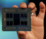
Source: Tom's Hardware
Add your own comment

71 Comments on AMD Zen 2 "Rome" MCM Pictured Up Close

#51
SIGSEGV
zomg, that's huge chip, I believe zen 2 will use a different socket :oops:
Posted on Reply
#52
bug
SIGSEGVzomg, that's huge chip, I believe zen 2 will use a different socket :oops:
If you meant Ryzen2, that will probably only have a couple CCX dies. And it would still be plenty.
Posted on Reply
#53
Vayra86
I gotta say this is seriously cool stuff. So much potential. So much scalability and so deviously simple.
Posted on Reply
#54
bug
Vayra86I gotta say this is seriously cool stuff. So much potential. So much scalability and so deviously simple.
This is anything but simple. With the IO off the main die, you have to fight additional latency. For the time being these are made in separate fab nodes (Zen2 refresh will most certainly make that IO chip 7nm as well) so power draw is probably all over the place. This is not simple, but the result of many engineers working to make stuff happen.
Posted on Reply
#55
Vya Domus
cdawallSo you have no idea what knights landing is.
Neither Intel as it turns out since they ceased development of the Xeon Phi line. That was a weird ass product for which the industry had no need as it stood in a obscure place between it's own many-core x86 CPUs and GPUs from Nvidia and AMD which obliterated it in terms of pref/watt and performance in general. Phi was yet another case of Intel's failure to grasp what the industry really needed and what they could deliver. No wonder really, after all it's birth took place because of the aftermath of yet another failed product: a dedicated GPU.
Posted on Reply
#56
HTC
Vya DomusNeither Intel as it turns out since they ceased development of the Xeon Phi line. That was a weird ass product for which the industry had no need as it stood in a obscure place between it's own many-core x86 CPUs and GPUs from Nvidia and AMD which obliterated it in terms of pref/watt and performance in general. Phi was yet another case of Intel's failure to grasp what the industry really needed and what they could deliver. No wonder really, after all it's birth took place because of the aftermath on yet another failed product: a dedicated GPU.
Not following: you quoted me ... with something i didn't say ... huh???
Posted on Reply
#57
Vya Domus
HTCNot following: you quoted me ... with something i didn't say ... huh???
Sorry, don't know how the hell did that happen.
Posted on Reply
#58
HTC
Vya DomusSorry, don't know how the hell did that happen.
I forgive you ... but only this one time ... and the next 100 ...
Posted on Reply
#59
WikiFM
Darmok N JaladWith the way it’s designed, I see different IO chips depending on the application. Base chips will likely have far fewer PCIe lanes, fewer memory channels, etc.
Seems likely, I would like to hear confirmation from AMD.
Posted on Reply
#60
TheoneandonlyMrK
WikiFMSeems likely, I would like to hear confirmation from AMD.
He's just repeating what I said earlier ,no consumer space news or info has been disclosed, but it's been hinted at that all of the next generation is pciex4 compatible so the io chip absolutely is , they would likely have used pciex 4 inter die and between the chip and io controller , there's the reason.
No more pciex3 or below on the ccx chip , likely just pciex 4 links and no memory controller and all using IF2 protocols.
So mainstream and below will require some level of backwards compatibility and an io chip , though it could be a old school north/south bridge stlye too in reality , not many know and they're tihht lipped but between comments and rumours lie truth ,see adoreds video on rome , he's a tool but he was right somehow.
Posted on Reply
#61
Valantar
cdawallI was implying with TR4 needing an update. Basing that in how the IO worked with the chip. If it is a carry over that'll be interesting that's for sure. AMD being able to basically completely change how the cpus are able to talk to each other, where the memory controllers are, where the pcie root complex is and using the exact same socket would be impressive.
I agree that it'd be impressive, but in the end, isn't the only thing necessary for socket compatibility in the sense you're talking about connecting the right wires from the right I/O to the right pads on the bottom of the substrate? As long as the engineers designing the substrate do their job properly to ensure signal integrity, the socket or connected components won't care how the on-package links are laid out. Your memory traces don't care if they're connected to a single I/O die or four dual-channel controllers on separate chips, after all.

Edit: oh ain't it fun when the forum decides to paste in the remnants of some discarded half-written post before posting what you just wrote. Sorry about that :p
Posted on Reply
#62
mtcn77
iO~70mm^2 per chiplet, ~440mm^2 for the I/O chip. Quite thicc, might suggest some form of L4$.
Suppose this is true, it would equal a 1000mm² chip - that is above the reticle limit and requires selective filling of the metal layers like their HBM interposers.
Posted on Reply
#63
TheoneandonlyMrK
ValantarYeah, I agree, if they have indeed moved to 8-core CCXes we'll likely see a

I agree that it'd be impressive, but in the end, isn't the only thing necessary for socket compatibility in the sense you're talking about connecting the right wires from the right I/O to the right pads on the bottom of the substrate? As long as the engineers designing the substrate do their job properly to ensure signal integrity, the socket or connected components won't care how the on-package links are laid out. Your memory traces don't care if they're connected to a single I/O die or four dual-channel controllers on separate chips, after all
They're are direct physical limitations that determine trace length maximums for memory and pciex, and memory and pciex lanes are now the main routings through a socket and could force change, but they say it's epyc compatible, yet has two more memory channels, it will be interesting to get details.
Posted on Reply
#64
Valantar
theoneandonlymrkThey're are direct physical limitations that determine trace length maximums for memory and pciex, and memory and pciex lanes are now the main routings through a socket and could force change, but they say it's epyc compatible, yet has two more memory channels, it will be interesting to get details.
Hm? EPYC has eight channel DDR4. TR has quad channel. As for the rest, increases in trace length ought to be negligible, given that - at most - they're moved from the "not quite in the corners" position of TR/EPYC to the "edge of this huge central die" position of the new I/O die. Given that this has been in the works for quite some time, since well before the launch of previous-gen chips, one would think they designed the TR4/SP4 pinouts to allow for this routing, no? If not, that would be a rather glaring oversight.
Posted on Reply
#65
TheoneandonlyMrK
ValantarHm? EPYC has eight channel DDR4. TR has quad channel. As for the rest, increases in trace length ought to be negligible, given that - at most - they're moved from the "not quite in the corners" position of TR/EPYC to the "edge of this huge central die" position of the new I/O die. Given that this has been in the works for quite some time, since well before the launch of previous-gen chips, one would think they designed the TR4/SP4 pinouts to allow for this routing, no? If not, that would be a rather glaring oversight.
yes that oversight was mine , brain fart for a mo i got them at 6 channels for epyc ,doh i actually did know that they had 8, honest :p:(
Posted on Reply
#66
Imsochobo
CheapMeatDo you think they put a large L4 cache on the center IO chip?
This could resolve many scenarios where increase in memory latency you get with chiplet design if any, I trust AMD not having any regressions in any scenario cause it'd be a suicide.
The real question, in what scenario's have they improved things and we Know:
Throughput.
Density.
Clock speed increase (25%)
Latency consistency.
IPC.
Scalability.
PCI-E G4.
Posted on Reply
#67
Valantar
ImsochoboThis could resolve many scenarios where increase in memory latency you get with chiplet design if any, I trust AMD not having any regressions in any scenario cause it'd be a suicide.
The real question, in what scenario's have they improved things and we Know:
Throughput.
Density.
Clock speed increase (25%)
Latency consistency.
IPC.
Scalability.
PCI-E G4.
True. We also know that they're calling the IF implementation "reduced latency IF", so even if we should expect some increase in RAM latency compared to previous latency on the Zeppelin-integrated controller, I'm not expecting it to be horrible. Might be optimistic of me, though. Still, for 1st gen TR AMD claimed 78ns latency for "near" memory and 133ns for "far" memory. If this is "latency reduced" IF (which it should be, as the link between any chiplet and the I/O die should be noticeably shorter than the link between any two Zeppelins in TR/EPYC 1st gen, and the memory access is only passing through a dedicated I/O die and not an actual logic die (even if off-die memory access of course wasn't processed by the CPU, there are likely optimizations to be done)), I'm hoping for overall memory latencies <100ns, though lower would be better.
Posted on Reply
#68
HD64G
AMD from a financial and marketing aspect they should make a single chiplet cpu for AM4 with a light igpu in it connecting those through the if. Power consumption will be minimal on 7nm after all. 8C/16T will be more than enough for any not enthusiast pc owner, especially if IPC is up by 15% and clocks get close to 5GHz for 1-2 threads. TR3 should have half of the EPYC cores and memory channels. Segmentation is very important for any company, especially when they try to take over the market with new and revolutionary products. And by doing this, price will be great for all since the small cpu for AM4 will be ultra cheap to make and super competitive to Intel offerings, TR is an enthusiast product and only those who have big money will bother and EPYC will win by brute force and lower consumption than Xeons. My 5 cents.
Posted on Reply
#69
Valantar
HD64GAMD from a financial and marketing ascect they should make a single chiplet cpu for AM4 with a light igpu in it connecting those through the if. Power consuption will be minimal on 7nm after all. 8C/16T will be more than enough for any not enthusiast pc owner, especially if IPC is up by 15% and clocks get close to 5GHz for 1-2 threads. TR3 should have half of the EPYC cores amd memory channels. Segmentation is very important for any company, especially when they try to take over the market with new and revolutionary products. And by doing this, price will be great for all since the small cpu for AM4 will be ultra cheap to make and super competitive to Intel offerings, TR is an enthusiast product and only those who have big money will bother and EPYC will win by brute force and lower consumption than Xeons. My 5 cents.
IMO, it would be baffling if AMD didn't do this exact thing. Heck, given that their PCIe controllers double as IF controllers, it should be trivial (insofar as anything in engineering a modern CPU can be called "trivial") for them to hook any off-the-shelf GPU die (given that they implement this PCIe architecture in their GPUs - I have no idea, but I can't imagine anything upcoming not doing this, at least) up to an I/O die over IF and pretty much call it a day. The IF linkup will give the GPU direct memory access, and a far faster uplink than PCIe - not to mention that it won't eat up the CPU's PCIe lanes unlike in Raven Ridge, as that's entirely decided by the I/O die.


Thought experiment: might we see specialised EPYC offshoots replacing half the CPU chiplets with GPU chiplets? Sure, they'll be memory starved when compared to any HBM2 or GDDR setup, but why not? Or might we see SKUs implementing HBM2 stacks in there too (4 CPU chiplets, 2 GPU chiplets and 2 stacks of HBM2?)? It shouldn't be too hard to run a HBM2 controller off the IF links in the I/O die, after all. Does anyone have an idea of the total bandwidth of a single IF link? Would a single 8-hi stack of 1024-bit 2000MT/s HBM2 saturate it?
Posted on Reply
#70
terroralpha
HD64GAMD from a financial and marketing aspect they should make a single chiplet cpu for AM4 with a light igpu in it connecting those through the if. Power consumption will be minimal on 7nm after all. .....
maybe sometimes far down the road, i'm sure they'd love to do that. but it's not going to happen any time soon because it's not up to AMD. 7nm is in large demand and AMD is very far down in the food chain of TSMC's customers. Apple takes about 20% of TSMC's output and if rumors are correct they may soon replace intel's CPUs with their own, which will naturally be made by TSMC, and will consume even more of TSMC's output. Qualcom is the second biggest customer followed by Nvidia and a few others. AMD is somewhere after that. so for now all the 7nm stuff will only be in EPYC and the high end GPUs.
Posted on Reply
#71
Valantar
terroralphamaybe sometimes far down the road, i'm sure they'd love to do that. but it's not going to happen any time soon because it's not up to AMD. 7nm is in large demand and AMD is very far down in the food chain of TSMC's customers. Apple takes about 20% of TSMC's output and if rumors are correct they may soon replace intel's CPUs with their own, which will naturally be made by TSMC, and will consume even more of TSMC's output. Qualcom is the second biggest customer followed by Nvidia and a few others. AMD is somewhere after that. so for now all the 7nm stuff will only be in EPYC and the high end GPUs.
Well, I'm not that worried. Nvidia doesn't have any 7nm products yet, and while they're no doubt working on datacenter 7nm stuff, it's not even announced yet. Consumer 7nm from Nvidia won't be coming for at least another year, given that Turing just launched on 12nm. Apple makes a lot of silicon sure, but as you say, that's around 20% of their capacity. Qualcomm is also huge, but they mainly make small chips, even in gigantic quantities. I'm reasonably sure AMD can squeeze in there without major issues. Not to mention the prestige for TSMC to be making chips for high-end servers, supercomputers and datacenters (even if they already do this for Nvidia, they haven't done CPUs before). And given the density improvements on 7nm, they should be able to reduce the number of wafers required for anyone producing small dice, freeing up capacity for AMD. Sure, there's going to be a squeeze between Apple, Nvidia, Qualcomm and AMD, and AMD is the smallest of the four, but ultimately there should be enough to go around, and it seems that AMD has been on the ball early enough to ensure a decent supply agreement. Fabbing the I/O die on GloFo 14nm is also a brilliant move, as it's a much larger die (at least for EPYC), on a cheaper node, mostly consisting of components that don't scale well with node shrinks anyhow (physical interconnects, possibly cache), meaning that it doesn't cannibalize 7nm fab capacity and wouldn't make sense on 7nm anyhow. Someone in the Zen 2 29% IPC thread calculated that AMD likely will get 600-900 good 8-core chiplets off a single 7nm wafer depending on yields. That bodes pretty well for reaching a good production volume even on a relatively immature process, and they wouldn't need that many wafer starts a month to sustain supply.
Posted on Reply
Add your own comment
Apr 26th, 2024 15:28 EDT change timezone

New Forum Posts

Popular Reviews

Controversial News Posts