Tuesday, November 6th 2018

AMD Zen 2 "Rome" MCM Pictured Up Close

Here is the clearest picture of AMD "Rome," codename for the company's next-generation EPYC socket SP3r2 processor, which is a multi-chip module of 9 chiplets (up from four). While first-generation EPYC MCMs (and Ryzen Threadripper) were essentially "4P-on-a-stick," the new "Rome" MCM takes the concept further, by introducing a new centralized uncore component called the I/O die. Up to eight 7 nm "Zen 2" CPU dies surround this large 14 nm die, and connect to it via substrate, using InfinityFabric, without needing a silicon interposer. Each CPU chiplet features 8 cores, and hence we have 64 cores in total.

The CPU dies themselves are significantly smaller than current-generation "Zeppelin" dies, although looking at their size, we're not sure if they're packing disabled integrated memory controllers or PCIe roots anymore. While the transition to 7 nm can be expected to significantly reduce die size, groups of two dies appear to be making up the die-area of a single "Zeppelin." It's possible that the CPU chiplets in "Rome" physically lack an integrated northbridge and southbridge, and only feature a broad InfinityFabric interface. The I/O die handles memory, PCIe, and southbridge functions, featuring an 8-channel DDR4 memory interface that's as monolithic as Intel's implementations, a PCI-Express gen 4.0 root-complex, and other I/O.
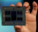
Source: Tom's Hardware
Add your own comment

71 Comments on AMD Zen 2 "Rome" MCM Pictured Up Close

#26
HTC
Question: any word on how stock markets are taking yersterday's event on both Intel and AMD?

Just wondering.
Posted on Reply
#27
bug
HTCQuestion: any word on how stock markets are taking yersterday's event on both Intel and AMD?

Just wondering.
AMD gained like 8% (iirc) on announcing their deal with Amazon. Intel's event hasn't happened yet.
Posted on Reply
#28
Vya Domus
FordGT90ConceptStill relevant:
Relevant indeed, after all Intel is now struggling with all their might to do the same. Gluing together dies and cutting Hyper-Threading in order to obtain an acceptable power envelope with a design clearly not meant to be scalable beyond it's initial conception.
Posted on Reply
#29
HTC
bugAMD gained like 8% (iirc) on announcing their deal with Amazon. Intel's event hasn't happened yet.
I was wondering about the Intel's / AMD's stock's current worth with respective ups / downs right after yesterday's presentation.
Posted on Reply
#30
bug
HTCI was wondering about the Intel's / AMD's stock's current worth with respective ups / downs right after yesterday's presentation.
Beyond that Amazon deal, this was too vague to make a lasting impression with investors imho.
Posted on Reply
#31
Valantar
TheLostSwede@Valantar I think you've lost your marbles, you keep going on about dice, what dice? Are your trying to say AMD is gambling here? Or maybe you need to get a new spell checker...
The plural of die can be either dice, die or dies. I prefer the former, as it's less confusing than the latter two (one is the same as the singular, and also a verb, while the other is a conjugation of said verb). Sure, it's also the same word as the thing used for craps and similar games, but at least that's still a noun, and even one with the same etymological origin. Just because nobody uses the singular "die" for one of the white thingies with black dots on the sides used for playing games doesn't mean that it's a different word, unlike the other two. Source.
londisteDo we have confirmation on this? As fas as I have seen, there have not been any details about the internals of Zen2.
Not yet, but given that every single other rumor concerning this has lined up so far, IMO it would be odd if this wasn't the case. Of course, it could still happen. But considering that inter-CCX latency was one of the first and most obvious performance limitations for Zen, it would be odd if they didn't seek to address that with Zen2.
Posted on Reply
#32
R0H1T
ValantarThe plural of die can be either dice, die or dies. I prefer the former, as it's less confusing than the latter two (one is the same as the singular, and also a verb, while the other is a conjugation of said verb). Sure, it's also the same word as the thing used for craps and similar games, but at least that's still a noun, and even one with the same etymological origin. Just because nobody uses the singular "die" for one of the white thingies with black dots on the sides used for playing games doesn't mean that it's a different word, unlike the other two. Source.


Not yet, but given that every single other rumor concerning this has lined up so far, IMO it would be odd if this wasn't the case. Of course, it could still happen. But considering that inter-CCX latency was one of the first and most obvious performance limitations for Zen, it would be odd if they didn't seek to address that with Zen2.
There's a small possibility that AMD could make two (or more) separate dies with different CCX layouts. One (IGP less) for pure CPU, like EPYC, with 8 cores per CCX & the other with 4 core per CCX & an IGP, the latter for mobile market. This is purely speculation, from my side, based on the assumption that any APU design with eight x86 cores will be OTT for ULP or ULV segments.

Of course it's entirely possible that we get a single CCX with 4 cores, to rule them all.
Posted on Reply
#33
iO
~70mm^2 per chiplet, ~440mm^2 for the I/O chip. Quite thicc, might suggest some form of L4$.
Posted on Reply
#34
the54thvoid
Intoxicated Moderator
Vya DomusRelevant indeed, after all Intel is now struggling with all their might to do the same. Gluing together dies and cutting Hyper-Threading in order to obtain an acceptable power envelope with a design clearly not meant to be scalable beyond it's initial conception.
That's a salient point. Intel have pushed the fabrication scale on a very solid design but that design cannot adapt very well. AMD had to approach their design from a fresh perspective and it's a gamble they had to take. Looks very much like it has paid dividends, literally.
I'm quite excited to see Zen 2.
Posted on Reply
#35
MDDB
R0H1TThere's a small possibility that AMD could make two (or more) separate dies with different CCX layouts. One (IGP less) for pure CPU, like EPYC, with 8 cores per CCX & the other with 4 core per CCX & an IGP, the latter for mobile market. This is purely speculation, from my side, based on the assumption that any APU design with eight x86 cores will be OTT for ULP or ULV segments.

Of course it's entirely possible that we get a single CCX with 4 cores, to rule them all.
Inside a CCX, every core has to be linked to every other core. Having 4 cores per CCX means there have to be 6 links established for this all-to-all communication. If they went with more than 4 cores per CCX, that number of links grows very quickly. 5 cores would require 10 links, 6 cores need 15 links, 7 cores need 21 links and 8 cores need 28 links: that's a huge amount of inter-core links, that would take lots of place and make the design innefficient. My guess, based on AMD's modular strategy, is that the CCX will remain at 4 cores, and that each new Zen 2 die still has two 4-cores CCXs. The inter CCXs latency will remain a thing, although hopefully IF2 will help.

Now that they have taken all I/O out of the zen dice (yes, i too say "dice", seems sensible), they can change the former strategy of having 2 designs: one die with 1 CCX and an iGPU for the Raven Ridge line, and another with 2 CCXs for everything else. Now they could have several chiplets connected via IF2 on the same substrate to serve different markets. So for example 1 Zen 2 die + I/O + iGPU for Picasso, 2 zen 2 dice + I/O for regular Ryzen 3xxx (no iGP), 4 zen 2 dice + I/O for Threadripper 3, and as seen yesterday 8 dice + I/O for Epyc 2. Only the I/O would have to change from one design to another, and not even, they might be able to just use two versions of the I/O die, one for TR & Epyc, one for Ryzen 3xxx (both Picasso and regular Ryzen).

In any case, i think an 8 cores CCX is out of question, out of pure complexity of the design. We'll see soon enough!
Posted on Reply
#36
Darmok N Jalad
WikiFMWill Rome be using dies from both TSMC(7 nm chiplets) and GF(14 nm I/O) right?
Also will less than 64 cores CPUs be using dummy or faulty silicon as before?
Also will the 2 dies next to each other communicate directly?
I don't think Ryzen 3000 will use the I/O die, since it is 14 nm and is huge and perhaps very expensive. That means that Rome either has IMC and PCI disabled, or more likely Ryzen will have a different die.
With the way it’s designed, I see different IO chips depending on the application. Base chips will likely have far fewer PCIe lanes, fewer memory channels, etc.
TheLostSwedeI don't know what AMD is planning with Ryzen 3xxx on the CPU side, but I have some insight on the chipset side of things.

First the bad news, motherboards are going to get even more expensive, as with PCIe 4.0 the boards are going to need some kind of "re-driver" for the PCIe 4.0 signals and apparently at least one is required, but if you want dual x16 slots on boards, supposedly two are needed. These are expensive parts and will increase board costs.

From my understanding, AMD is going full-on PCIe 4.0, so not only the lanes from the CPU to the chipset will be PCIe 4.0, but also the lanes to all peripherals. This means AMD will be the first company to offer full PCIe 4.0 support on a consumer board, unless Intel can get something out before the Ryzen 3xxx series launches. Expect a vastly improved chipset, but I can't reveal too much as yet, as I don't want to get people in trouble for leaking information that isn't even remotely public as yet. All I can say is that I think everyone will be a lot happier with AMD's high-end chipset for the Ryzen 3xxx series, as it doesn't have any of the weird limitations that the current chipsets have. There won't be any bandwidth starved peripherals this time around.
But won’t the IO chip now be on the CPU package? The motherboard could get very simple in other places, largely becoming just a base for different devices to plug into. I guess this one redriver might be all that’s needed, and we’re going to see some changes to where plugs are found on boards?
Posted on Reply
#37
micgre8162
The CPU chiplets will house PCIE 4.0 lanes. The memory controllers are being moved to the I/O die. I think this is a good move for AMD. We already see Intel following the MCM path with their glued 48 core Xeon thing. I'm not sure where they're going with that, but most likely Intel is working within the limits of their 14nm process.

Assuming they don't fall on their faces at launch, and this is AMD so that can't be ruled out, this looks like a very promising technology.
Posted on Reply
#38
R0H1T
MDDBInside a CCX, every core has to be linked to every other core. Having 4 cores per CCX means there have to be 6 links established for this all-to-all communication. If they went with more than 4 cores per CCX, that number of links grows very quickly. 5 cores would require 10 links, 6 cores need 15 links, 7 cores need 21 links and 8 cores need 28 links: that's a huge amount of inter-core links, that would take lots of place and make the design innefficient. My guess, based on AMD's modular strategy, is that the CCX will remain at 4 cores, and that each new Zen 2 die still has two 4-cores CCXs. The inter CCXs latency will remain a thing, although hopefully IF2 will help.

Now that they have taken all I/O out of the zen dice (yes, i too say "dice", seems sensible), they can change the former strategy of having 2 designs: one die with 1 CCX and an iGPU for the Raven Ridge line, and another with 2 CCXs for everything else. Now they could have several chiplets connected via IF2 on the same substrate to serve different markets. So for example 1 Zen 2 die + I/O + iGPU for Picasso, 2 zen 2 dice + I/O for regular Ryzen 3xxx (no iGP), 4 zen 2 dice + I/O for Threadripper 3, and as seen yesterday 8 dice + I/O for Epyc 2. Only the I/O would have to change from one design to another, and not even, they might be able to just use two versions of the I/O die, one for TR & Epyc, one for Ryzen 3xxx (both Picasso and regular Ryzen).

In any case, i think an 8 cores CCX is out of question, out of pure complexity of the design. We'll see soon enough!
Sure about that?


If they added as much as 32(?) MB L3 then the CCX will have to be redesigned, it's entirely plausible that the same core layout was reused but there are other major changes as well which we'll find out about eventually.
Posted on Reply
#39
micgre8162
WikiFMWill Rome be using dies from both TSMC(7 nm chiplets) and GF(14 nm I/O) right?
Also will less than 64 cores CPUs be using dummy or faulty silicon as before?
Also will the 2 dies next to each other communicate directly?
I don't think Ryzen 3000 will use the I/O die, since it is 14 nm and is huge and perhaps very expensive. That means that Rome either has IMC and PCI disabled, or more likely Ryzen will have a different die.
The point of using the I/O on a larger die is that it can be fabricated on an older, and much less expensive, process. I'm a bit curious why AMD chose to use the GloFo 14nm instead of the TSMC 16nm and keep everything in TSMC's shop. I'd love to hear AMD talk about that.
Posted on Reply
#40
HTC
MDDBInside a CCX, every core has to be linked to every other core. Having 4 cores per CCX means there have to be 6 links established for this all-to-all communication. If they went with more than 4 cores per CCX, that number of links grows very quickly. 5 cores would require 10 links, 6 cores need 15 links, 7 cores need 21 links and 8 cores need 28 links: that's a huge amount of inter-core links, that would take lots of place and make the design innefficient. My guess, based on AMD's modular strategy, is that the CCX will remain at 4 cores, and that each new Zen 2 die still has two 4-cores CCXs. The inter CCXs latency will remain a thing, although hopefully IF2 will help.

Now that they have taken all I/O out of the zen dice (yes, i too say "dice", seems sensible), they can change the former strategy of having 2 designs: one die with 1 CCX and an iGPU for the Raven Ridge line, and another with 2 CCXs for everything else. Now they could have several chiplets connected via IF2 on the same substrate to serve different markets. So for example 1 Zen 2 die + I/O + iGPU for Picasso, 2 zen 2 dice + I/O for regular Ryzen 3xxx (no iGP), 4 zen 2 dice + I/O for Threadripper 3, and as seen yesterday 8 dice + I/O for Epyc 2. Only the I/O would have to change from one design to another, and not even, they might be able to just use two versions of the I/O die, one for TR & Epyc, one for Ryzen 3xxx (both Picasso and regular Ryzen).

In any case, i think an 8 cores CCX is out of question, out of pure complexity of the design. We'll see soon enough!
The topology they use will be key: so far, we know nothing about the topology being used but for Zen 2's Ryzen, i suspect it will be "butterdonut" topology.

Read the following:

NoC Architectures for Silicon Interposer Systems (PDF file) for context, and Enabling Interposer-based Disintegration of Multi-core Processors (PDF file).

Both of these require an interposer so dunno exactly how they do it. Perhaps this will come only with Zen 3? Dunno.
Posted on Reply
#41
londiste
micgre8162We already see Intel following the MCM path with their glued 48 core Xeon thing. I'm not sure where they're going with that, but most likely Intel is working within the limits of their 14nm process.
Intel's current LCC and HCC CPUs do not have enough UPI links, XCC has three which is why it is the only one they can use for gluing at this time.
Posted on Reply
#43
TheoneandonlyMrK
MDDBInside a CCX, every core has to be linked to every other core. Having 4 cores per CCX means there have to be 6 links established for this all-to-all communication. If they went with more than 4 cores per CCX, that number of links grows very quickly. 5 cores would require 10 links, 6 cores need 15 links, 7 cores need 21 links and 8 cores need 28 links: that's a huge amount of inter-core links, that would take lots of place and make the design innefficient. My guess, based on AMD's modular strategy, is that the CCX will remain at 4 cores, and that each new Zen 2 die still has two 4-cores CCXs. The inter CCXs latency will remain a thing, although hopefully IF2 will help.

Now that they have taken all I/O out of the zen dice (yes, i too say "dice", seems sensible), they can change the former strategy of having 2 designs: one die with 1 CCX and an iGPU for the Raven Ridge line, and another with 2 CCXs for everything else. Now they could have several chiplets connected via IF2 on the same substrate to serve different markets. So for example 1 Zen 2 die + I/O + iGPU for Picasso, 2 zen 2 dice + I/O for regular Ryzen 3xxx (no iGP), 4 zen 2 dice + I/O for Threadripper 3, and as seen yesterday 8 dice + I/O for Epyc 2. Only the I/O would have to change from one design to another, and not even, they might be able to just use two versions of the I/O die, one for TR & Epyc, one for Ryzen 3xxx (both Picasso and regular Ryzen).

In any case, i think an 8 cores CCX is out of question, out of pure complexity of the design. We'll see soon enough!
I agree but think at the bottom end that could be too expensive a Bom ie a 2ccx chiplet an io chip and gpu, the io is over the top for mainstream and below so how about a second io chip , smaller and combined with a gpu on die, that could make sense or the io will be replicated on and still in a ccx ,fir mainstream and below.
Posted on Reply
#45
TheLostSwede
News Editor
Darmok N JaladBut won’t the IO chip now be on the CPU package? The motherboard could get very simple in other places, largely becoming just a base for different devices to plug into. I guess this one redriver might be all that’s needed, and we’re going to see some changes to where plugs are found on boards?
No, those are not the same thing. The one that's part of the CPU package is for the main PCIe lanes from the CPU and the memory controller, it has nothing to do with things like peripheral connectivity, so a chipset is still needed. The information I got is from a very reliable source, so don't expect any huge board design changes for now. The issue with the re-driver is because PCIe 4.0 loses signal integrity over even fairly short distances. This should help explain the technical limitations a bit better eecatalog.com/pcie/2018/03/20/the-high-frequency-signals-of-pcie-4-0-demand-higher-performance-from-engineers/
Posted on Reply
#46
cdawall
where the hell are my stars
ValantarAMD stated plainly that Rome is socket compatible with previous-gen EPYC. So no
I was implying with TR4 needing an update. Basing that in how the IO worked with the chip. If it is a carry over that'll be interesting that's for sure. AMD being able to basically completely change how the cpus are able to talk to each other, where the memory controllers are, where the pcie root complex is and using the exact same socket would be impressive.
narayani don't care about other projects, my dear friend, all i care about are CPUs and GPUs
because of the past 10 yrs and intel's "good consumer policies", i just hate them, truly hate them

PS: let's not forget how and what intel did to AMD for reaching a now shaking 1 position
So you have no idea what knights landing is. Gotcha, you could have just said that.
Posted on Reply
#47
TheGuruStud
cdawallSo you have no idea what knights landing is. Gotcha, you could have just said that.
Another intel failure.
Posted on Reply
#48
MDDB
R0H1TThose aren't IF links just so you know.
I never said so, because i don't know what type of connection is used; the important thing is that there is some kind of connection, of link, and that adding cores to a CCX would multiply the number of such connections.
Posted on Reply
#50
Space Lynx
Astronaut
I really can't wait for summer/winter 2019 and 7nm AMD CPU and GPU. Might be my last silicon build as I plan to go back to consoles for future AAA releases when Playstation 5 comes out.
Posted on Reply
Add your own comment
Apr 26th, 2024 06:58 EDT change timezone

New Forum Posts

Popular Reviews

Controversial News Posts