Friday, December 6th 2019

TSMC on Track to Deliver 3 nm in 2022

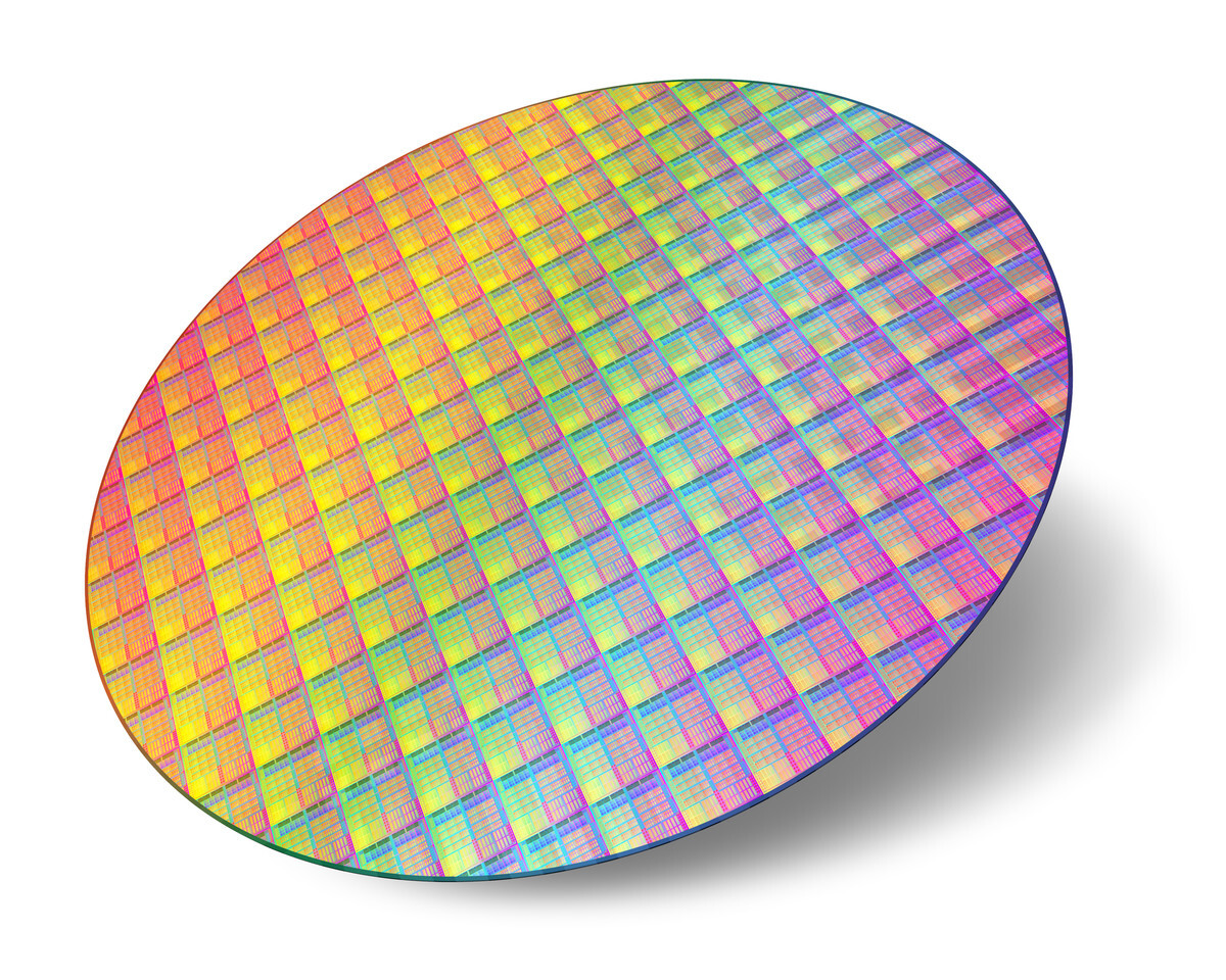
TSMC is delivering record results day after day, with a 5 nm manufacturing process starting High Volume Manufacturing (HVM) in Q2 next year, 7 nm process getting plenty of orders and the fact that TSMC just became the biggest company publicly trading in Asia. Continuing with the goal to match or even beat the famous Moore's Law, TSMC is already planning for future 3 nm node manufacturing, promised to start HVM as soon as 2022 arrives, according to JK Wang, TSMC's senior vice president of fab operations. Delivering 3 nm a whole year before originally planned in 2023, TSMC is working hard, with fab construction work doing quite well, judging by all the news that the company is releasing recently.

We can hope to see the first wave of products built using 3 nm manufacturing process sometime around end of year 2022, when the holiday season arrives. Usual customers like Apple and HiSilicon will surely utilize the new node and deliver their smartphones with 3 nm processors inside as soon as the process is ready for HVM.
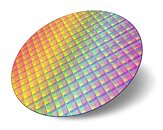
Source: DigiTimes
Add your own comment

71 Comments on TSMC on Track to Deliver 3 nm in 2022

#1
Vayra86
Seeing is believing, until the chips are on shelf and not scarce, its not a reality.

After all, between flooding, viruses and the occasional fire, 2022 is very far away.
Posted on Reply
#2
Space Lynx
Astronaut
Vayra86Seeing is believing, until the chips are on shelf and not scarce, its not a reality.

After all, between flooding, viruses and the occasional fire, 2022 is very far away.
the occasional fire, made me laugh. that flood in Thailand that hurt the Hard Drive market for a solid 3-5 years... hope it doesn't happen again
Posted on Reply
#3
medi01
I recall GloFo was right on track or better with 7nm, right up to the point when it wasn't.

Let's see how 5nm rolls out in 2021.
Posted on Reply
#4
notb
Their 5nm is not even what we were going to call 7nm few years ago.
But just look at the progress! 7, 5, 3! Unbelievable.

They could have just called it TURBO, MAX or MEGA.
Posted on Reply
#5
fancucker
So Zen 4 will be on 5nm/+? Papermeister needs those new nodes for moar coars to circumvent that pesky moore's law and avoid the possibility of willow/golden cove finally arriving
Posted on Reply
#6
ppn
Navi delivers 40 Mtr, and ZEN2 50 Mtr/mm2 density. 7nm DUV is supposed to be 90. so there is more improvement to be made on 7nm by adding more layers, 5 now, 14 on 5nm. Considering that normally for 14nm the numbers are 25 and 30. So 3nm with 14 layers will be a beast. And still be less dense than intels 5nm. Time will show.
Posted on Reply
#7
ratirt
fancuckerSo Zen 4 will be on 5nm/+? Papermeister needs those new nodes for moar coars to circumvent that pesky moore's law and avoid the possibility of willow/golden cove finally arriving
Unbelievable. You've got no boundaries man :)
ppnNavi delivers 40 Mtr, and ZEN2 50 Mtr/mm2 density. 7nm DUV is supposed to be 90. so there is more improvement to be made on 7nm by adding more layers, 5 now, 14 on 5nm. Considering that normally for 14nm the numbers are 25 and 30. So 3nm with 14 layers will be a beast. And still be less dense than intels 5nm. Time will show.
So is the 6nm process node scrapped? I thought TSMC is developing the 6nm as well.
Posted on Reply
#8
notb
ratirtSo is the 6nm process node scrapped? I thought TSMC is developing the 6nm as well.
6nm is 7nm++.
It's all just a marketing name by now.
It's just a waste of time that gamers got pulled into this so easily. No one cares about important stuff anymore.
Posted on Reply
#9
londiste
ppnNavi delivers 40 Mtr, and ZEN2 50 Mtr/mm2 density. 7nm DUV is supposed to be 90. so there is more improvement to be made on 7nm by adding more layers, 5 now, 14 on 5nm. Considering that normally for 14nm the numbers are 25 and 30. So 3nm with 14 layers will be a beast. And still be less dense than intels 5nm. Time will show.
Thing with that is, there are multiple processes in the 7nm family. A low-power process that usually gets used for SoCs and whatnot that actually clocks in close to or at that 90 Mtr/mm^2 and a high performance variation that gets half of the density but clocks a lot higher. This is of course simplified and there are more variations for some manufacturing processes and less for others but that is the gist of it. Same applies to 12/14/16nm and earlier ones as well.

Adding EUV layers has little to do with performance and usually not that much with power efficiency. It is all about manufacturing, both ease/accuracy and speed of it. Both of these have implications for performance but are not done directly for that.
Posted on Reply
#10
ratirt
notb6nm is 7nm++.
It's all just a marketing name by now.
It's just a waste of time that gamers got pulled into this so easily. No one cares about important stuff anymore.
Yeah i do realize now it is just marketing. Read extensive articles about it but if you use these 7nm 6nm EUV DUV whatever freely, you tend to loose grip on what's going on and what these actually represent.
There are few different 7nm processes and it is just confusing now.
Posted on Reply
#11
Flanker
ratirtYeah i do realize now it is just marketing. Read extensive articles about it but if you use these 7nm 6nm EUV DUV whatever freely, you tend to loose grip on what's going on and what these actually represent.
There are few different 7nm processes and it is just confusing now.
That time when Samsung's "14nm" node turned out to be much more power hungry than TSMC's 16nm node (it was Apple A9 chip I believe), I stopped caring about the nm numbers lol. I have to have some benchmarks reviews.
Posted on Reply
#12
fancucker
ratirtYeah i do realize now it is just marketing. Read extensive articles about it but if you use these 7nm 6nm EUV DUV whatever freely, you tend to loose grip on what's going on and what these actually represent.
There are few different 7nm processes and it is just confusing now.
notb6nm is 7nm++.
It's all just a marketing name by now.
It's just a waste of time that gamers got pulled into this so easily. No one cares about important stuff anymore.
6nm isn't 7nm+. Its a half-node shrink that gets the same EUV benefits but is fully design rule compatible with 7nm. Its basically a cheaper solution for the higher demand until 5nm
Posted on Reply
#13
ratirt
FlankerThat time when Samsung's "14nm" node turned out to be much more power hungry than TSMC's 16nm node (it was Apple A9 chip I believe), I stopped caring about the nm numbers lol. I have to have some benchmarks reviews.
I guess that is reasonable. Wait and see what the node gives when the products are out.
Posted on Reply
#14
Super XP
TSMC already proven themselves with 7nm. I am sure they will successfully come out with 5nm and 3nm all in time for future RDNA & ZEN releases.
Posted on Reply
#15
notb
fancucker6nm isn't 7nm+. Its a half-node shrink that gets the same EUV benefits but is fully design rule compatible with 7nm. Its basically a cheaper solution for the higher demand until 5nm
It's just a marketing name. These nanometers have no physical meaning.

6nm will be an improved (more dense) 7nm+. Just like 7nm+ is improved (more dense) 7nm - despite still being called "7".
5nm will be a new design.

It's free market and these values aren't regulated (like e.g. 1 gram is, so you're not allowed to sell smaller chocolate bars because your "gram" is smaller).

There's an informal, industry standard for naming (ITRS/IRDS) and if we looked at that, TSMC's 7nm is almost exactly ITRS's 10nm. Again: TSMC's 5nm is more like "industry 7nm".
But since TSMC could change the naming and look more advanced, they did.
It seems they're stepping back a bit lately, with their product names shifting to the Nx notation. 7nm became N7, 7nm++ is N6 etc.
But as I said: they could just use any idiotic naming like "Ti BOOST" or "EPYC".

Adidas makes a shoe called "AlphaEdge 4D Shoe - Star Wars" and hell yeah, I want that!
Posted on Reply
#16
Super XP
I agree it's marketing. That's what companies use is strategic naming to make it sound good. But 7nm+ is also an advanced process method. In this respect the actual name is justified.
Posted on Reply
#17
notb
Super XPI agree it's marketing. That's what companies use is strategic naming to make it sound good. But 7nm+ is also an advanced process method. In this respect the actual name is justified.
Absolutely. No one is trying to say TSMC's 7nm is not advanced. It's the most advanced mass-production node we have today.
That being said, if TSMC stayed with the IRDS naming, this would be called 10nm, so it would launch just few months before Intel's.
But calling it 7nm makes the impression that they're leading by 3 years.
And they're already announcing "5nm" and "3nm" as if they've found a spaceship full of unknown technology. :)
Posted on Reply
#18
bug
Vayra86Seeing is believing, until the chips are on shelf and not scarce, its not a reality.

After all, between flooding, viruses and the occasional fire, 2022 is very far away.
It's the Pacific Rim, why rule out earthquakes?
But the news is about TSMC being where they wanted to be now, not in 2022 or any year in between.
Posted on Reply
#19
LFaWolf
@AleksandarK as I have posted in the other article, Tencent Holding from China, is listed on the Hang Seng Stock Exchange (HKSE), has a market cap of $3.2T in Hong Kong Dollars. Converting to USD, that is over $400B USD. How can TSM be the largest publicly traded company in Asia? Where is your source?
www.bloomberg.com/quote/700:HK
Posted on Reply
#20
notb
LFaWolf@AleksandarK as I have posted in the other article, Tencent Holding from China, is listed on the Hang Seng Stock Exchange (HKSE), has a market cap of $3.2T in Hong Kong Dollars. Converting to USD, that is over $400B USD. How can TSM be the largest publicly traded company in Asia? Where is your source?
www.bloomberg.com/quote/700:HK
Alibaba's market cap is over $500B.
Tencent is second. TSMC may be third at best.
Posted on Reply
#21
iO
And at the same time Intel revives a 22nm CPU from 2013 because they can't even get their 10nm to work properly.

PCN 117291-01 (pdf)
"Intel(R) Pentium(R) Processor G3420 (3M Cache, 3.20 GHz) FC-LGA12C, Tray, PCN 117291-01, Product Discontinuance, End of Life, Reason for Revision: Cancelling this Product Discontinuance completely per new roadmap decision and enabling the product once again."
Posted on Reply
#22
LFaWolf
notbAlibaba's market cap is over $500B.
Tencent is second. TSMC may be third at best.
In the other article, the writer mentioned it is for company listed on the Asia stock exchange. Alibaba has a smaller market cap listing in Asia, but Tencent is listed solely in Asia, and I know Tencent market cap in Asia is close to Alibaba listing in USA. I just don’t see how TSMC or TT (its stock symbol on Taiwan stock exchange) can be larger than Tencent holding
Posted on Reply
#23
HugsNotDrugs
A mere 3nm is around the size of a single molecule.

The end-of-the-line for silicon is near.
Posted on Reply
#24
notb
@AleksandarK
"biggest company publicly trading in Asia"
Should be "publicly traded in Asia", but wording is still not ideal.
"biggest company listed on an Asian stock exchange" would be precise.

And as mentioned by @LFaWolf, it's at best second largest.
Posted on Reply
#25
Vayra86
bugIt's the Pacific Rim, why rule out earthquakes?
But the news is about TSMC being where they wanted to be now, not in 2022 or any year in between.
Yes, the article reads a lot like Intel's 10nm 'going according to plan', you're correct about that. Where did I read such things before? Oh yeah, every shrink since 22nm :D

But you're right, earthquakes, and let's not forget climate change either.
Posted on Reply
Add your own comment
Apr 27th, 2024 05:37 EDT change timezone

New Forum Posts

Popular Reviews

Controversial News Posts