Monday, April 12th 2021

NVIDIA Announces Grace CPU for Giant AI and High Performance Computing Workloads
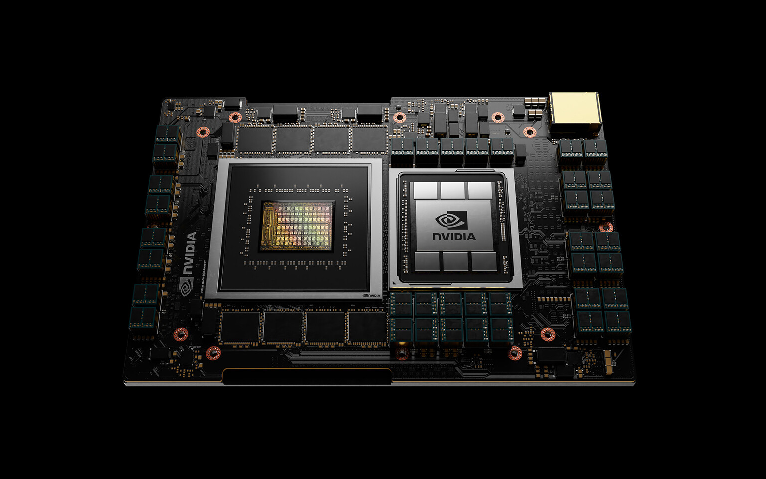
NVIDIA today announced its first data center CPU, an Arm-based processor that will deliver 10x the performance of today's fastest servers on the most complex AI and high performance computing workloads.
The result of more than 10,000 engineering years of work, the NVIDIA Grace CPU is designed to address the computing requirements for the world's most advanced applications—including natural language processing, recommender systems and AI supercomputing—that analyze enormous datasets requiring both ultra-fast compute performance and massive memory. It combines energy-efficient Arm CPU cores with an innovative low-power memory subsystem to deliver high performance with great efficiency. "Leading-edge AI and data science are pushing today's computer architecture beyond its limits - processing unthinkable amounts of data," said Jensen Huang, founder and CEO of NVIDIA. "Using licensed Arm IP, NVIDIA has designed Grace as a CPU specifically for giant-scale AI and HPC. Coupled with the GPU and DPU, Grace gives us the third foundational technology for computing, and the ability to re-architect the data center to advance AI. NVIDIA is now a three-chip company."
Grace is a highly specialized processor targeting workloads such as training next-generation NLP models that have more than 1 trillion parameters. When tightly coupled with NVIDIA GPUs, a Grace CPU-based system will deliver 10x faster performance than today's state-of-the-art NVIDIA DGX -based systems, which run on x86 CPUs.
While the vast majority of data centers are expected to be served by existing CPUs, Grace—named for Grace Hopper, the U.S. computer-programming pioneer—will serve a niche segment of computing.
The Swiss National Supercomputing Centre (CSCS) and the U.S. Department of Energy's Los Alamos National Laboratory are the first to announce plans to build Grace-powered supercomputers in support of national scientific research efforts.
NVIDIA is introducing Grace as the volume of data and size of AI models are growing exponentially. Today's largest AI models include billions of parameters and are doubling every two-and-a-half months. Training them requires a new CPU that can be tightly coupled with a GPU to eliminate system bottlenecks.
NVIDIA built Grace by leveraging the incredible flexibility of Arm's data center architecture. By introducing a new server-class CPU, NVIDIA is advancing the goal of technology diversity in AI and HPC communities, where choice is key to delivering the innovation needed to solve the world's most pressing problems.
"As the world's most widely licensed processor architecture, Arm drives innovation in incredible new ways every day," said Arm CEO Simon Segars. "NVIDIA's introduction of the Grace data center CPU illustrates clearly how Arm's licensing model enables an important invention, one that will further support the incredible work of AI researchers and scientists everywhere."
Grace's First Adopters Push Limits of Science and AI
CSCS and Los Alamos National Laboratory both plan to bring Grace-powered supercomputers, built by Hewlett Packard Enterprise, online in 2023.
"NVIDIA's novel Grace CPU allows us to converge AI technologies and classic supercomputing for solving some of the hardest problems in computational science," said CSCS Director Prof. Thomas Schulthess. "We are excited to make the new NVIDIA CPU available for our users in Switzerland and globally for processing and analyzing massive and complex scientific datasets."
"With an innovative balance of memory bandwidth and capacity, this next-generation system will shape our institution's computing strategy," said Thom Mason, director of the Los Alamos National Laboratory. "Thanks to NVIDIA's new Grace CPU, we'll be able to deliver advanced scientific research using high-fidelity 3D simulations and analytics with datasets that are larger than previously possible."
Delivering Breakthrough Performance
Underlying Grace's performance is fourth-generation NVIDIA NVLink interconnect technology, which provides a record 900 GB/s connection between Grace and NVIDIA GPUs to enable 30x higher aggregate bandwidth compared to today's leading servers.
Grace will also utilize an innovative LPDDR5x memory subsystem that will deliver twice the bandwidth and 10x better energy efficiency compared with DDR4 memory. In addition, the new architecture provides unified cache coherence with a single memory address space, combining system and HBM GPU memory to simplify programmability.
Grace will be supported by the NVIDIA HPC software development kit and the full suite of CUDA and CUDA-X libraries, which accelerate more than 2,000 GPU applications, speeding discoveries for scientists and researchers working on the world's most important challenges.
Availability is expected in the beginning of 2023.
The result of more than 10,000 engineering years of work, the NVIDIA Grace CPU is designed to address the computing requirements for the world's most advanced applications—including natural language processing, recommender systems and AI supercomputing—that analyze enormous datasets requiring both ultra-fast compute performance and massive memory. It combines energy-efficient Arm CPU cores with an innovative low-power memory subsystem to deliver high performance with great efficiency.
Grace is a highly specialized processor targeting workloads such as training next-generation NLP models that have more than 1 trillion parameters. When tightly coupled with NVIDIA GPUs, a Grace CPU-based system will deliver 10x faster performance than today's state-of-the-art NVIDIA DGX -based systems, which run on x86 CPUs.
While the vast majority of data centers are expected to be served by existing CPUs, Grace—named for Grace Hopper, the U.S. computer-programming pioneer—will serve a niche segment of computing.
The Swiss National Supercomputing Centre (CSCS) and the U.S. Department of Energy's Los Alamos National Laboratory are the first to announce plans to build Grace-powered supercomputers in support of national scientific research efforts.
NVIDIA is introducing Grace as the volume of data and size of AI models are growing exponentially. Today's largest AI models include billions of parameters and are doubling every two-and-a-half months. Training them requires a new CPU that can be tightly coupled with a GPU to eliminate system bottlenecks.
NVIDIA built Grace by leveraging the incredible flexibility of Arm's data center architecture. By introducing a new server-class CPU, NVIDIA is advancing the goal of technology diversity in AI and HPC communities, where choice is key to delivering the innovation needed to solve the world's most pressing problems.
"As the world's most widely licensed processor architecture, Arm drives innovation in incredible new ways every day," said Arm CEO Simon Segars. "NVIDIA's introduction of the Grace data center CPU illustrates clearly how Arm's licensing model enables an important invention, one that will further support the incredible work of AI researchers and scientists everywhere."
Grace's First Adopters Push Limits of Science and AI
CSCS and Los Alamos National Laboratory both plan to bring Grace-powered supercomputers, built by Hewlett Packard Enterprise, online in 2023.
"NVIDIA's novel Grace CPU allows us to converge AI technologies and classic supercomputing for solving some of the hardest problems in computational science," said CSCS Director Prof. Thomas Schulthess. "We are excited to make the new NVIDIA CPU available for our users in Switzerland and globally for processing and analyzing massive and complex scientific datasets."
"With an innovative balance of memory bandwidth and capacity, this next-generation system will shape our institution's computing strategy," said Thom Mason, director of the Los Alamos National Laboratory. "Thanks to NVIDIA's new Grace CPU, we'll be able to deliver advanced scientific research using high-fidelity 3D simulations and analytics with datasets that are larger than previously possible."
Delivering Breakthrough Performance
Underlying Grace's performance is fourth-generation NVIDIA NVLink interconnect technology, which provides a record 900 GB/s connection between Grace and NVIDIA GPUs to enable 30x higher aggregate bandwidth compared to today's leading servers.
Grace will also utilize an innovative LPDDR5x memory subsystem that will deliver twice the bandwidth and 10x better energy efficiency compared with DDR4 memory. In addition, the new architecture provides unified cache coherence with a single memory address space, combining system and HBM GPU memory to simplify programmability.
Grace will be supported by the NVIDIA HPC software development kit and the full suite of CUDA and CUDA-X libraries, which accelerate more than 2,000 GPU applications, speeding discoveries for scientists and researchers working on the world's most important challenges.
Availability is expected in the beginning of 2023.
13 Comments on NVIDIA Announces Grace CPU for Giant AI and High Performance Computing Workloads
Bigger is better, right?
The picture doesn't even look like what they're describing a server Cpu, it looks like the latest jetsun no Orin (latest model released today too called errrrrrrrrrrrr, ATLAN)self driving module not a CPU, which is listed on another site I won't name and also uses grace cores With a GPU attached on a board just like that one.
I feel this product may face strong headwinds because most big companies are deploying their own ARM custom SOC that supposedly suits their workload, and it is likely also cheaper. So unless Nvidia's acquisition of ARM goes through and they start gimping other users of ARM SOC which I believe will be the case soon or later, I am not sure how well they will sell this.
When the average consumer can't get a 1650 Super for less than 300€ in 2021 it's pitiful and shows that the corporation doesn't give a damn.