Monday, August 23rd 2021

Samsung Develops 512 GB DDR5 Memory Modules Running at 7.2 Gbps
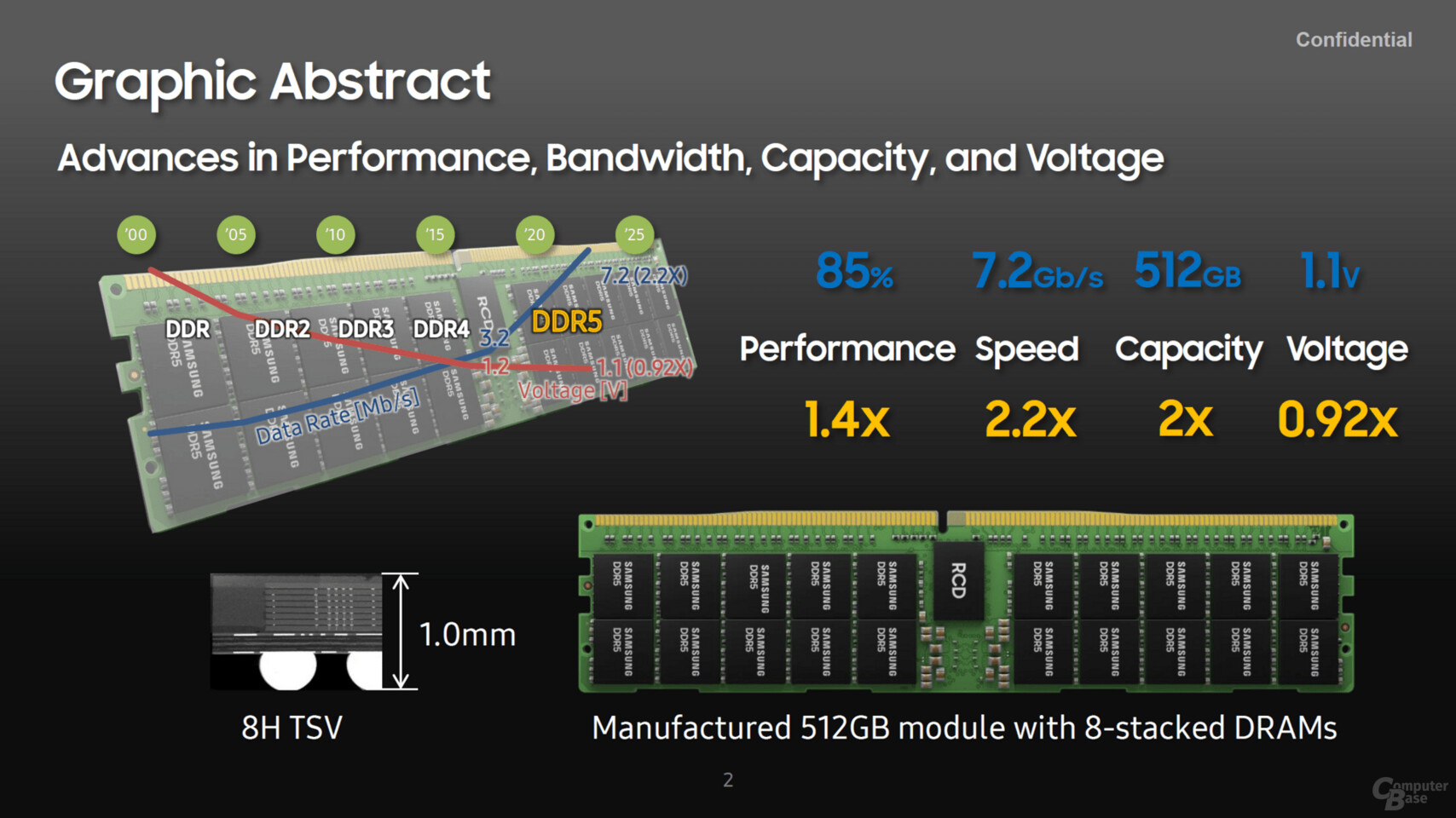
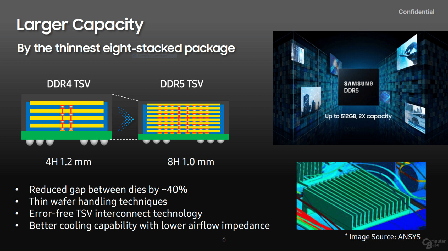
At this year's Hot chips 33 conference, Samsung has presented its works on the upcoming DDR5 memory standard. The company has managed to achieve a lot of new developments, as the newer standard pairs with new technologies to deliver higher speeds and better capacity. The Korean company designed its DDR5 modules as 8-high (8H) stacked TSV (through silicon via) dies. In the previous DDR4 implementations, Samsung used 4-high (4H) stacked TSV dies, which are actually thicker than the latest 8-high implementations. To achieve the new thin design, Samsung has used thin wafer handling techniques, which resulted in a 40% reduction in gab between stacked dies. The new 8H DDR5 modules are only 1.0 mm thick, compared to the 1.2 mm of the older 4H modules.
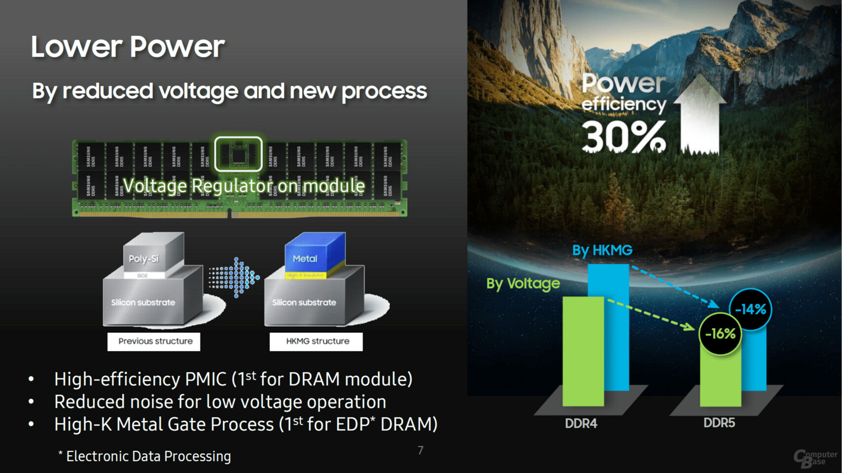
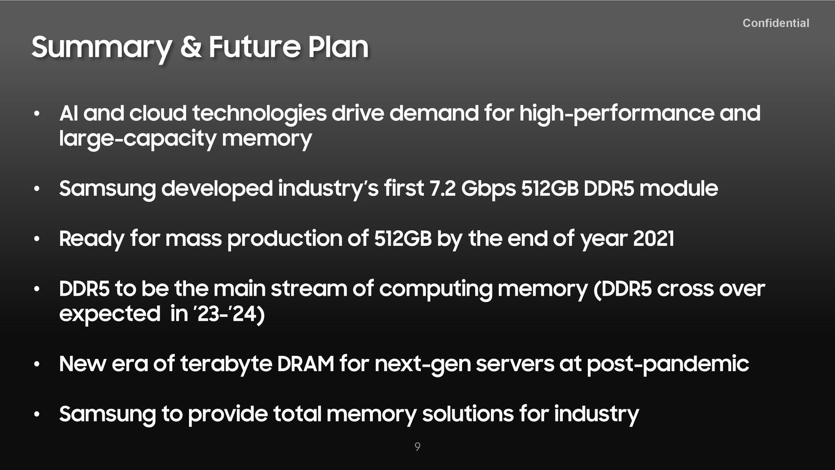
When it comes to performance, Samsung expects the new DDR5 modules to deliver big. Running at 7.2 Gbps speeds, the Samsung-made RDIMM/LRDIMM modules can reach up to 512 GB in capacity. This is, of course, limited to the server/enterprise market. Regular consumers/PC users can expect to have UDIMMs with up to 64 GB of capacity. The aforementioned 7.2 Gbps speed is achieved at the specified 1.1 Volts of power, meaning that Samsung's implementation is very efficient. According to some estimations made by the company, the DDR5 crossover for the mainstream market is not expected before 2023/2024, meaning that there is still a lot of time for memory makers to refine their DDR5 products.


Sources:
ComputerBase, via VideoCardz
When it comes to performance, Samsung expects the new DDR5 modules to deliver big. Running at 7.2 Gbps speeds, the Samsung-made RDIMM/LRDIMM modules can reach up to 512 GB in capacity. This is, of course, limited to the server/enterprise market. Regular consumers/PC users can expect to have UDIMMs with up to 64 GB of capacity. The aforementioned 7.2 Gbps speed is achieved at the specified 1.1 Volts of power, meaning that Samsung's implementation is very efficient. According to some estimations made by the company, the DDR5 crossover for the mainstream market is not expected before 2023/2024, meaning that there is still a lot of time for memory makers to refine their DDR5 products.
27 Comments on Samsung Develops 512 GB DDR5 Memory Modules Running at 7.2 Gbps
GDDR6, on the other hand, can operate either at double or quad data rate (the latter requires halving the clock frequency, WCK). Check out this document from Micron, page 11.
Anyone (old enough) want to calculate the baud rates?
Baud rate in this case should be half the bit rate (10GBaud for GDDR6X 20Gb/s).