Friday, August 15th 2025

Intel Showcases Reference Arm-based SoC Manufactured on 18A Node

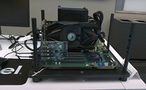
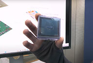
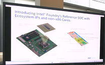
Intel Foundry has been releasing content on its products and services, and today, an interesting update came across. Intel showed a reference "Deer Creek Falls" SoC of what they call a "non-x86" design, manufactured on the 18A node. However, the design is actually Arm-based SoC. Consisting of seven cores, the reference SoC packs a single performance core, two efficiency cores, and four low-power efficiency cores, alongside the embedded PCIe and memory controller IPs and PHYs from ecosystem partners. While this may not be an impressive design, it demonstrates that a heterogeneous design of hybrid cores and IPs from ecosystem partners exists, and it's likely that we will see some designs emerging from this.

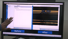
While Intel didn't explicitly mention that this SoC is Arm, later in the video, in the section on performance tuning, there are mentions of AArch64, which is Arm's designation for the 64-bit Arm ISA flavor. Alongside the design, Intel also demonstrated that the company offers a suite of performance optimization tools, even for Arm-based processors, allowing its customers to optimize and enhance software performance on their preferred platform, not just the x86 ISA. Hopefully, external foundry customers are slowly becoming aware of Intel Foundry's capabilities, and the scale can commence, especially now that Intel is under supervision from the U.S. government.

14:10 UTC: Update: Intel has delisted the video from its YouTube channel, but our screenshots remain.
While the 18A node showed little interest for external customers, Intel plans to use it extensively across its product lines. For 14A, Intel has evaluated switching its approach and evaluating if customers want to utilize it first, then build more 14A capacity. However, that plan is likely scrapped, and Intel will continue leading-edge node development unconditionally. There are already reports of companies like Apple and NVIDIA evaluating Intel's 14A node, so the Foundry could finally catch some momentum. As the U.S. government also showed interest, we can expect to see many more designs going through the gates of Intel Foundry in the coming quarters.
Add your own comment

26 Comments on Intel Showcases Reference Arm-based SoC Manufactured on 18A Node

#1
kondamin
Just release a new batch of small cheap atom processors made on the node while maturing it GDMT!!!!!!!!!!!!
Posted on Reply
#2
Vayra86
Fan Fucking Tastic Intel, you doing all these cool things in them sweet labs.

But we all know your new nodes are one big clusterbeep and you're just postponing the inevitable here.
Posted on Reply
#3
mb194dc
Back to the pumping we go, until the next quarters financial results anyway ?

Nvidia next ?
Posted on Reply
#4
TheLostSwede
News Editor
That has to be the physically biggest Arm chip ever made, including the packaging.
This really looks nuts and even the physical size of the IC is really weird.
Posted on Reply
#5
Igb
Just about 1-2 weeks ago some news sites published the intention of Intel to mostly skip 18A in favour of 14A citing low yields.

Now this piece of news hints to the exact opposite.

I know they must keep the investors happy but all these weird changes of mind smell really bad.
Posted on Reply
#6
Rightness_1
Nobody cares about 18A, all eyes are on 14A - This will make or break Intel once and for all.
Posted on Reply
#7
Igb
Rightness_1Nobody cares about 18A, all eyes are on 14A - This will make or break Intel once and for all.
They said the same, word for word, regarding 18A like half a year ago. It is Groundhog day all over again
Posted on Reply
#8
vmetodiev
The video has just become no longer available...?
Posted on Reply
#9
MufasaV
IgbJust about 1-2 weeks ago some news sites published the intention of Intel to mostly skip 18A in favour of 14A citing low yields.

Now this piece of news hints to the exact opposite.

I know they must keep the investors happy but all these weird changes of mind smell really bad.
Intel never said anything about yields. They are focusing RnD in getting the support systems, DTCO and tooling right for 14A having missed 18A window for fast movers

About yields, ask Reuters who think an entire architecture lineup is being launched with 10% yields (or not being launched at all contrary to Intel claims).
Posted on Reply
#10
Tomorrow
TheLostSwedeThat has to be the physically biggest Arm chip ever made, including the packaging.
This really looks nuts and even the physical size of the IC is really weird.
That chip looks miniscule on that interposer/PCB. Most likely a marketing stunt.
So Intel can produce a simple, small, working ARM chip on 18A? [insert: slow clap]
This tells us nothing.

Even showing a prototype 18A based Nova Lake running stable would not tell us much, because ultimately the yields have been the bane of Intel's in-house nodes.
Posted on Reply
#11
TheLostSwede
News Editor
TomorrowThat chip looks miniscule on that interposer/PCB. Most likely a marketing stunt.
It's still massive compared to your average Arm chip, but as we don't even know what cores are being used, it's hard to tell how much bigger it is.
Posted on Reply
#12
Tomorrow
TheLostSwedeIt's still massive compared to your average Arm chip, but as we don't even know what cores are being used, it's hard to tell how much bigger it is.
What is an "average" ARM chip size? From the image it looks like two skinny Zen chiplets stacked side by side judging from the proportions of the human hand.
2xZen 5 are 141,2mm².

SnapDragon X1E is 169,6mm²
Apple M series chips are in the 150-170mm² range too.

At least if were comparing laptop/mini-PC chips.
ARM based smartphone chips are obviously smaller at around or below 100mm², but that's not a proportional comparison as the form factor is completely different.

I would say it's pretty average for a laptop class ARM chip.
Posted on Reply
#13
TheLostSwede
News Editor
TomorrowWhat is an "average" ARM chip size? From the image it looks like two skinny Zen chiplets stacked side by side judging from the proportions of the human hand.
2xZen 5 are 141,2mm².

SnapDragon X1E is 169,6mm²
Apple M series chips are in the 150-170mm² range too.

At least if were comparing laptop/mini-PC chips.
ARM based smartphone chips are obviously smaller at around or below 100mm², but that's not a proportional comparison as the form factor is completely different.

I would say it's pretty average for a laptop class ARM chip.
Yeah, those are laptop grade chips and far from your average Arm chip, which would be something like that in your phone or router.
These are a few years old, but where typical phone chips at the time.
Whatever Intel made, is clearly bigger than these.
The second picture suggests four energy efficient cores, one high performance core, two PCIe controllers and four memory controllers, plus something I can't quite read, but it seems to be two performance cores maybe? So no graphics, no modem, no WiFi/Bluetooth, no DSP, plus a bunch of other things the chips below have, which explains the graphics card and USB host controller card in the third picture.

Posted on Reply
#14
tfp
kondaminJust release a new batch of small cheap atom processors made on the node while maturing it GDMT!!!!!!!!!!!!
You mean ecore only processors?
Posted on Reply
#15
Denver
TheLostSwedeYeah, those are laptop grade chips and far from your average Arm chip, which would be something like that in your phone or router.
These are a few years old, but where typical phone chips at the time.
Whatever Intel made, is clearly bigger than these.
The second picture suggests four energy efficient cores, one high performance core, two PCIe controllers and four memory controllers, plus something I can't quite read, but it seems to be two performance cores maybe? So no graphics, no modem, no WiFi/Bluetooth, no DSP, plus a bunch of other things the chips below have, which explains the graphics card and USB host controller card in the third picture.

Must be a server chip, Ampere Altra die is larger than 500mm².
Posted on Reply
#16
Operandi
Yeah.... they made single (performance) core server CPU in 2025🙄.

Seriously, there is something very weird about the proportions of this die for what it supposed to be. Makes you wonder if the picture has anything to do with this news story.
Posted on Reply
#17
TheLostSwede
News Editor
DenverMust be a server chip, Ampere Altra die is larger than 500mm².
With a total of seven cores?
OperandiYeah.... they made single (performance) core server CPU in 2025🙄.

Seriously, there is something very weird about the proportions of this die for what it supposed to be. Makes you wonder if the picture has anything to do with this news story.
It does line up with the weird Intel diagram though.
Posted on Reply
#18
kondamin
tfpYou mean ecore only processors?
Yes, small cheap energy sipping perfect for entry level windows 11 machines.
Posted on Reply
#19
sudothelinuxwizard
I'm hoping this will be an average-good performing SoC with good Linux support, because that's what Qualcomm's is missing.
Posted on Reply
#20
kondamin
sudothelinuxwizardI'm hoping this will be an average-good performing SoC with good Linux support, because that's what Qualcomm's is missing.
I doubt it’s coming to market, it’s a demo to show off hier foundry services.
Probably only made a limited run of the chip
Posted on Reply
#21
TheLostSwede
News Editor
sudothelinuxwizardI'm hoping this will be an average-good performing SoC with good Linux support, because that's what Qualcomm's is missing.
This is a foundry manufacturing ability demo, it's not a product, it's a pitch to get clients.
Posted on Reply
#22
Essaudio
The pitch is to show third party IP blocks being integrated with heterogeneous Arm cores on a recent node with optimization capabilities, supposedly. Honestly, this more than what I thought was possible right now from intel non x86, and that’s the point of the demo - I’m probably in the same boat as others who thought they were not ready to take real third party SoC orders and this doesn’t prove they are, but it’s something.
Posted on Reply
#23
igormp
TheLostSwedeThat has to be the physically biggest Arm chip ever made, including the packaging.
This really looks nuts and even the physical size of the IC is really weird.
Nvidia's Grace and Ampere Altra's CPU would like a word with you


With that said, both of these pack way more stuff than what Intel is presenting, so a bigger size is a given.
Posted on Reply
#25
Denver
TheLostSwedeWith a total of seven cores?


It does line up with the weird Intel diagram though.
I didn't notice that the specs were in the article. But it could well be an ARM SoC with a big GPU like the ones Nvidia uses.
Posted on Reply
Add your own comment
Nov 14th, 2026 17:26 CST change timezone

New Forum Posts

Popular Reviews

TPU on YouTube

Controversial News Posts