Wednesday, March 11th 2026

Intel Launches "Arrow Lake Refresh": Core Ultra 5 250K Plus and Core Ultra 7 270K Plus, New Binary Optimization Tool
Intel today announced the Core Ultra 5 250K Plus and Core Ultra 7 270K Plus desktop processors in the Socket LGA1851 package. These chips are drop-in compatible with existing Intel 800-series chipset motherboards, with some boards needing UEFI firmware updates. Both chips are based on the current "Arrow Lake" microarchitecture, and are carved out of the "Arrow Lake-S" disaggregated silicon that uses TSMC N3B (3 nm) foundry node for its Compute tile containing the CPU cores, TSMC N5 (5 nm) for its Graphics tile, and TSMC N6 (6 nm) node for its SoC and I/O tiles.
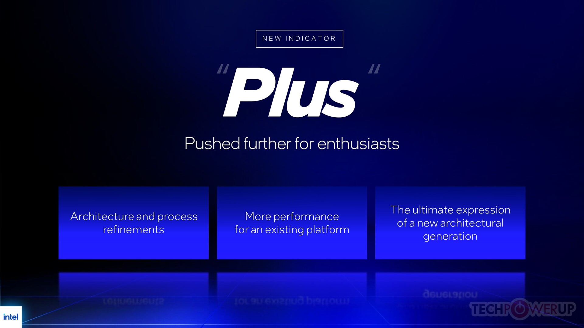
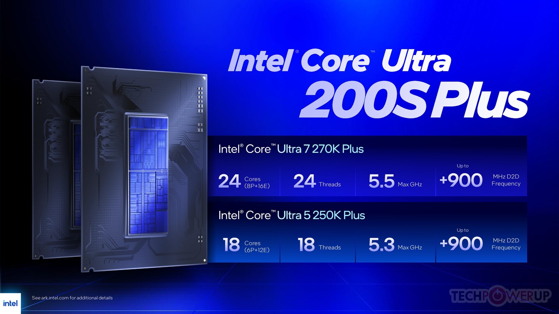
Both the Core Ultra 5 250K Plus ($199) and Core Ultra 7 270K Plus ($299) processor models are designed to push the current Core Ultra 5 245K and Core Ultra 7 265K, respectively, down from their current price-points. The two come with increased E-core counts, larger L3 caches, slightly increased P-core maximum boost frequency, and a 900 MHz faster die-to-die I/O frequency among the Compute and SoC tiles, which essentially makes these chips have "200S Boost Mode" out of the box. The new Core Ultra 5 250K Plus comes with a 6P+12E core configuration compared to the 6P+8E of the Core Ultra 5 245K. Its shared L3 cache has been enlarged to 30 MB, up from the 24 MB on the 245K. The P-core maximum boost frequency is up to 5.30 GHz from 5.20 GHz.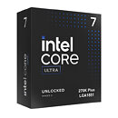
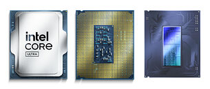
 Meanwhile, the Core Ultra 7 270K Plus maxes out the "Arrow Lake-S" silicon, enabling all 8 P-cores, and all 16 E-cores, along with the entire 36 MB of L3 cache present on the silicon. In comparison, the 265K only comes with an 8P+12E core configuration, with 30 MB of shared L3 cache. The only things segmenting the 270K Plus from the Core Ultra 9 285K are a lack of Thermal Velocity Boost algorithm, and a maximum P-core boost frequency of 5.50 GHz, compared to 5.70 GHz of the 285K. While it lacks Thermal Velocity Boost, it features Turbo Boost Max 3.0, just like the 265K does.
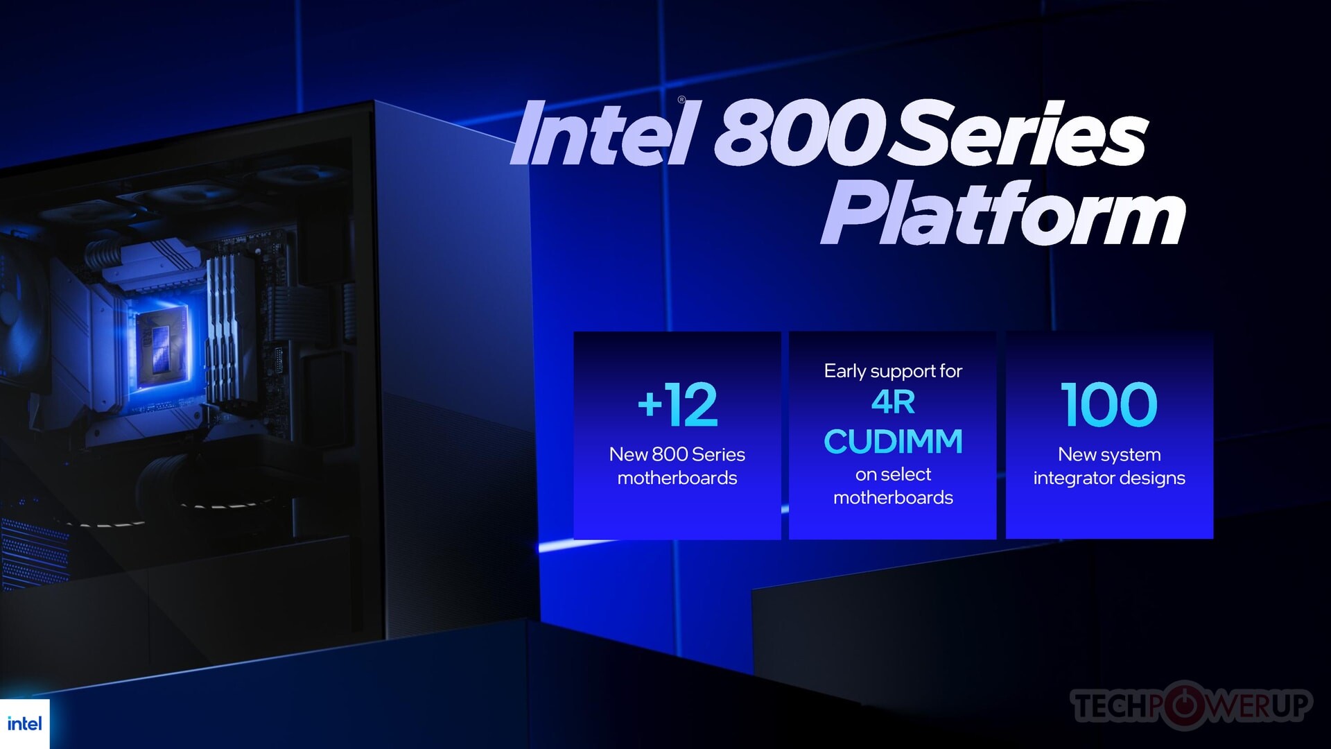
The Core Ultra 5 250K Plus and Core Ultra 7 270K Plus come with native support for DDR5-7200 memory speed, an increase from the DDR5-6400 native support of the older "Arrow Lake" desktop chips. Product warranty covers memory overclocking up to DDR5-8000. The two new chips also come with native support for quad-rank DDR5 CUDIMMs. These are new-generation UDIMMs that feature four DDR5 ranks and a client clock driver (CKD), helping consumer memory manufacturers significantly dial up densities along with memory speeds without having to use expensive high-density DRAM chips that are in short-supply. 4-rank CUDIMM support will also require motherboard vendors to implement it on their end with their latest products. It also requires certain UEFI firmware-level readiness.
Intel also announced the Binary Optimization Tool, a utility that helps end-users optimize application/game binaries to get the most performance out of "Arrow Lake-S" processors, we will have more details on that in our review later this month.
As mentioned earlier, the Core Ultra 5 250K Plus and Core Ultra 7 270K Plus are intended to displace the 245K and 265K, respectively, from their current price points. Both chips will begin retailing from March 26, 2026 for $199 and $299.
The full Intel presentation deck follows

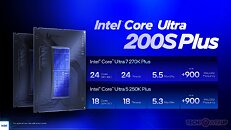
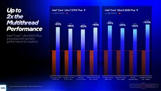
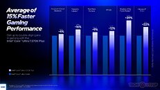
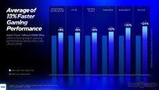









Both the Core Ultra 5 250K Plus ($199) and Core Ultra 7 270K Plus ($299) processor models are designed to push the current Core Ultra 5 245K and Core Ultra 7 265K, respectively, down from their current price-points. The two come with increased E-core counts, larger L3 caches, slightly increased P-core maximum boost frequency, and a 900 MHz faster die-to-die I/O frequency among the Compute and SoC tiles, which essentially makes these chips have "200S Boost Mode" out of the box. The new Core Ultra 5 250K Plus comes with a 6P+12E core configuration compared to the 6P+8E of the Core Ultra 5 245K. Its shared L3 cache has been enlarged to 30 MB, up from the 24 MB on the 245K. The P-core maximum boost frequency is up to 5.30 GHz from 5.20 GHz.


The Core Ultra 5 250K Plus and Core Ultra 7 270K Plus come with native support for DDR5-7200 memory speed, an increase from the DDR5-6400 native support of the older "Arrow Lake" desktop chips. Product warranty covers memory overclocking up to DDR5-8000. The two new chips also come with native support for quad-rank DDR5 CUDIMMs. These are new-generation UDIMMs that feature four DDR5 ranks and a client clock driver (CKD), helping consumer memory manufacturers significantly dial up densities along with memory speeds without having to use expensive high-density DRAM chips that are in short-supply. 4-rank CUDIMM support will also require motherboard vendors to implement it on their end with their latest products. It also requires certain UEFI firmware-level readiness.
Intel also announced the Binary Optimization Tool, a utility that helps end-users optimize application/game binaries to get the most performance out of "Arrow Lake-S" processors, we will have more details on that in our review later this month.
As mentioned earlier, the Core Ultra 5 250K Plus and Core Ultra 7 270K Plus are intended to displace the 245K and 265K, respectively, from their current price points. Both chips will begin retailing from March 26, 2026 for $199 and $299.
The full Intel presentation deck follows







59 Comments on Intel Launches "Arrow Lake Refresh": Core Ultra 5 250K Plus and Core Ultra 7 270K Plus, New Binary Optimization Tool
Back near release, I could either spend $250 on a 13600K system, or $500+ on a Core Ultra 5 245K system. DDR4 was also 3x cheaper than DDR5 at that time. This was when the Intel 13th and 14th Gen CPU's were having some... issues. Doing my research, the 13600K's default VCore was around 1.25V, while the 13700K and 13900K was around 1.45V's.
I cared about H.265 encoding:
A little bit of gaming (this is at 1080P):
Excel (or anything database related):
Potential for overclocking:
I'm able to get up to 5.7GHz - 5.4GHz with my 13600K at 1.35V's, compared to 5.5GHz for the Core Ultra 5 245K nearing 1.4V's. After getting two more 13600K's at an even lower price, I can confirm all three overclock to 5.7GHz easily on a 360 AIO at 1.35V's.
Paying 2x to 3x more for a new CPU model compared to 2 generations back model that performs slightly worse in every aspect I'm looking for, didn't make sense.
This is just me holding Intel's feet to the fire, since I do the same with AMD and NVIDIA.
Yes, P/E core isn't ideal, but Skymont IPC is almost the same as the last gen Raptor Cove P-cores. Windows being bad with it isn't Intel's fault (okay it kind of is, but Linux does it flawlessly AFAIK).
And besides, we should be welcoming this bone being thrown at us during this horrible DRAM crisis, however small it is. $299 MSRP for a downclocked 285k is just insane, even if with the DRAM crisis it's just average value.
The moment you throw in something that breaks those principles (like asymmetric CPU cores), you have to make specific tweaks to ensure programs aren't negatively impacted.
Imagine you were told all your life that you could throw your program on any "CPU" because the assumption that any "CPU" had the same performance (I put "CPU" in quotes because the program doesn't really care what it really is other than it's a "CPU"). But now with bit.LITTLE, whatever Intel's doing, and AMD's X3D and c variants, that assumption no longer holds true. And developers don't want to have applications figuring out what kind of hardware is running on the system and scheduling themselves.
Maybe there could be an application API or some such where the OS can say if it has asymmetric cores and the developer can flag threads as "high performance" or whatever, but then I'd imagine developers would just flag every thread as high performance because their application is the bestest in the world and only deserves to run on P-cores.
From an alleged press release I found:
It was my philosophy to wait over a year before jumping to a new platform, let all the bios & chipset drivers get sorted with bugs ironed out mostly to this point in time. Will I update to Nova Lake? way too early to speculate & even then so what if I have to change boards, PC building & tweaking is a hobby to me, that's the price (pardon the pun) you pay for interesting fun n' stuff.
It depends on games you played and when you played them, as the Windows 11 scheduler was gradually improved over the years. Even games like No Man's Sky that had this problem three years ago now run fine with no tinkering required. This was a big deal. There is a reason Bitsum released free Core Director and why motherboard manufacturers added "Legacy Game Mode" to their BIOSes that disables E-Cores with a key press. They would not have bothered if this wasn't an issue.
Seems to be paying off considering Intel is almost certainly not selling these at a loss, yet the P+E is competitive with P+P of 9950X, at ~half the price. Some of that is due to market pressure, since $500 eight core X3D chips that also carry the Zen name top low resolution gaming benchmarks with $3000 GPUs, so people seem to assume that applies to the entire Zen lineup, but it is what it is.
A few generations down the line, the rumour is the unified core design, which will allow similar cores to specialise in different targets in performance and efficiency, will be based off the E cores, not the P cores. So the back to the drawing board approach worked well for next gen parts.
Apple has just introduced a M core, between their super and their efficient. I guess they know what they're doing too, considering they're not just the performance and efficiency leader, but in a twist of fate, the value leader, too.