Thursday, April 9th 2026

Intel Foundry Combines GaN and Silicon Semiconductors on a Single Thin Chip
Intel Foundry has been delivering some interesting research lately, and the newest installment is the world's thinnest gallium nitride (GaN) chiplet, with the base silicon measuring just 19 micrometers in thickness. The company manufactured a 300-millimeter GaN-on-silicon wafer, which is one of the first combinations of GaN with traditional silicon logic on a single chip. In traditional manufacturing setups, GaN is reserved for power electronics and is not mixed with silicon-based computational logic. However, Intel has managed to combine GaN semiconductors for power delivery with silicon-based compute logic, meaning that power chips can now perform basic computations and actions on their own, without needing a separate chip to dictate behavior.
Intel manufactured the GaN wafer with silicon combined on the 30 nm process, which reportedly demonstrated excellent properties. This includes stable current carrying, very low power loss, and the ability to block voltages up to 78 V without leakage. What is fascinating is that GaN is usually used for wide bandgap applications, with high radio frequency performance exceeding 300 GHz. GaN also provides much better power delivery due to its superior material properties and operates more stably at higher temperatures. This is especially significant for workloads like electric vehicles or data center point-of-load delivery, where space is limited, temperatures can reach about 150°C, and stability is crucial.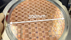
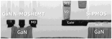
 Finally, Intel used a combination of traditional logic elements like inverters, NAND gates, multiplexers, ring oscillators, and more, all of which have been tested. The electrical properties of these circuits met the latest standards, achieving switching times of just 33 picoseconds, or 33 trillionths of a second, consistently across the entire 300 mm wafer that Intel produced. The new technology is proving to be promising due to its electrical properties, yield, and performance. Intel can potentially manufacture this at scale, which means we could see many future robotics and AI data center components integrating these chips.
Source:
Intel Foundry
Intel manufactured the GaN wafer with silicon combined on the 30 nm process, which reportedly demonstrated excellent properties. This includes stable current carrying, very low power loss, and the ability to block voltages up to 78 V without leakage. What is fascinating is that GaN is usually used for wide bandgap applications, with high radio frequency performance exceeding 300 GHz. GaN also provides much better power delivery due to its superior material properties and operates more stably at higher temperatures. This is especially significant for workloads like electric vehicles or data center point-of-load delivery, where space is limited, temperatures can reach about 150°C, and stability is crucial.


12 Comments on Intel Foundry Combines GaN and Silicon Semiconductors on a Single Thin Chip
I'm curious if that would translate over to logic circuits. Will we have another 2000s-style clock speed dick measuring contest with GaN-based CPUs?
hdplex.com/hdplex-fanless-250w-gan-aio-atx-psu.html
hdplex.com/hdplex-500w-gan-aio-atx-power-supply.html
There used to be a guy on the SFF forums who modded them up to 500 watt but he hasnt posted in years now.
So I wouldn’t be surprised if someday all CPUs and GPUs switch to higher voltages by drastically lowering the amperage to make things run cooler.
The main advantage of GaN is its super-fast switching speed, which in this case allows for smaller power supplies: the higher the frequency, the smaller the magnetics (transformers) become.
It takes time for a voltage to drop and it takes less time to go from 1v to 0v a clock cycle. Than it would from say 24v to 0v.
Chips do binary operations but operate on analog principles