Report an Error


ATI M98

M98
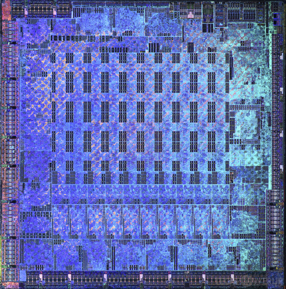
Die Shot

Block Diagram
ATI's M98 GPU uses the TeraScale architecture and is made using a 55 nm production process at TSMC. With a die size of 256 mm² and a transistor count of 956 million it is a medium-sized chip. M98 supports DirectX 10.1 (Feature Level 10_1). For GPU compute applications, OpenCL version 1.1 can be used. It features 800 shading units, 40 texture mapping units and 16 ROPs.
Further reading:
R700 Series Instruction Set Architecture 
Graphics Processor
- Released
- Jan 9th, 2009
- GPU Name
- M98
- Desktop Variant
- RV770
- Architecture
- TeraScale
- Foundry
- TSMC
- Process Size
- 55 nm
- Transistors
- 956 million
- Density
- 3.7M / mm²
- Die Size
- 256 mm²
- Package
- HFCBGA-1492
- Codename
- Wekiva
Graphics Features
- DirectX
- 10.1 (10_1)
- OpenGL
- 3.3
- OpenCL
- 1.1
- Vulkan
- N/A
- Shader Model
- 4.1
- WDDM
- 1.1
- Compute
- GFX3
- DCE
- 3.1
- UVD
- 2.0
Render Config
- Shading Units
- 800
- TMUs
- 40
- ROPs
- 16
- Compute Units
- 10
- Z-Stencil
- 64
- L1 Cache
- 16 KB per CU
- L2 Cache
- 256 KB
All TeraScale GPUs
- ATI M72
- ATI M74
- ATI M76
- ATI M82
- ATI M84
- ATI M86
- ATI M88
- ATI M92
- AMD M93
- ATI M93
- ATI M96
- ATI M97
- ATI M98
- ATI R600
- ATI R680
- ATI R700
- ATI RS780
- ATI RS880
- ATI RV610
- ATI RV620
- ATI RV630
- ATI RV635
- ATI RV670
- AMD RV670
- ATI RV710
- AMD RV711
- ATI RV711
- ATI RV730
- ATI RV740
- ATI RV770
- AMD RV770
- ATI RV790
- ATI RX881
- ATI Theater 650 PRO
- ATI Xenos Corona
- ATI Xenos Falcon
- ATI Xenos Jasper
- ATI Xenos Vejle
- ATI Xenos Xenon
ATI GPU Architecture History
Graphics cards using the ATI M98 GPU
| Name | Chip | Memory | Shaders | TMUs | ROPs | GPU Clock | Memory Clock |
|---|---|---|---|---|---|---|---|
| M98 L2 | 1024 MB | 800 | 40 | 16 | 503 MHz | 850 MHz | |
| M98 XT L2 | 512 MB | 800 | 40 | 16 | 550 MHz | 888 MHz | |
| M98 XT L2 | 1024 MB | 800 | 40 | 16 | 550 MHz | 700 MHz | |
| M98 L2 | 1024 MB | 800 | 40 | 16 | 500 MHz | 700 MHz | |
| M98 L2 | 512 MB | 800 | 40 | 16 | 503 MHz | 850 MHz |


M98 GPU Notes
| Desktop Variant: RV770 Codename: Wekiva Graphics/Compute: GFX3 Display Core Engine: 3.1 Unified Video Decoder: 2.0 Chip Codes: 216-0732000 - M98 A11 216-0732019 - M98 A12 216-0732004 - M98 XT A11 216-0732023 - M98 XT A12 |
Apr 26th, 2024 14:36 EDT
change timezone
Latest GPU Drivers
New Forum Posts
- hacked (74)
- Best SSD for system drive (87)
- looking to build a new system and im considering asrock brand but i have some doubts/concerns. (0)
- What phone you use as your daily driver? And, a discussion of them. (1485)
- XFX RX470 8GB no video and error 43 (29)
- DTS:X APO4 + DTS Interactive for Most Devices [USB Supported] (305)
- The Official Linux/Unix Desktop Screenshots Megathread (702)
- What's your latest tech purchase? (20352)
- im new to throttelstop and i think i messed it up by copying others any hints would be very much aprreciated (5)
- 2022-X58/1366 PIN Motherboards NVME M.2 SSD BIOS MOD Collection (657)
Popular Reviews
- HYTE THICC Q60 240 mm AIO Review
- MOONDROP x Crinacle DUSK In-Ear Monitors Review - The Last 5%
- Alienware Pro Wireless Gaming Keyboard Review
- Upcoming Hardware Launches 2023 (Updated Feb 2024)
- Thermalright Phantom Spirit 120 EVO Review
- FiiO K19 Desktop DAC/Headphone Amplifier Review
- ASUS Radeon RX 7900 GRE TUF OC Review
- AMD Ryzen 7 7800X3D Review - The Best Gaming CPU
- RTX 4090 & 53 Games: Ryzen 7 5800X vs Ryzen 7 5800X3D Review
- NVIDIA RTX 4090: 450 W vs 600 W 12VHPWR - Is there any notable performance difference?
Controversial News Posts
- Windows 11 Now Officially Adware as Microsoft Embeds Ads in the Start Menu (129)
- Sony PlayStation 5 Pro Specifications Confirmed, Console Arrives Before Holidays (117)
- NVIDIA Points Intel Raptor Lake CPU Users to Get Help from Intel Amid System Instability Issues (106)
- AMD "Strix Halo" Zen 5 Mobile Processor Pictured: Chiplet-based, Uses 256-bit LPDDR5X (103)
- US Government Wants Nuclear Plants to Offload AI Data Center Expansion (98)
- AMD's RDNA 4 GPUs Could Stick with 18 Gbps GDDR6 Memory (93)
- Developers of Outpost Infinity Siege Recommend Underclocking i9-13900K and i9-14900K for Stability on Machines with RTX 4090 (85)
- Windows 10 Security Updates to Cost $61 After 2025, $427 by 2028 (84)