Report an Error


ATI M76

M76

M76-M

M76 XT-M
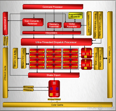
Block Diagram
ATI's M76 GPU uses the TeraScale architecture and is made using a 65 nm production process at TSMC. With a die size of 153 mm² and a transistor count of 390 million it is a small chip. M76 supports DirectX 10.0 (Feature Level 10_0). For GPU compute applications, OpenCL version N/A can be used. It features 120 shading units, 8 texture mapping units and 4 ROPs.
Further reading:
R600 Series Instruction Set Architecture 
Graphics Processor
- Released
- May 14th, 2007
- GPU Name
- M76
- Desktop Variant
- RV630
- Codename
- Shaka
- Architecture
- TeraScale
- Foundry
- TSMC
- Process Size
- 65 nm
- Transistors
- 390 million
- Density
- 2.5M / mm²
- Die Size
- 153 mm²
- Package
- FCBGA-880
Graphics Features
- DirectX
- 10.0 (10_0)
- OpenGL
- 3.3
- OpenCL
- N/A
- Vulkan
- N/A
- Shader Model
- 4.0
- WDDM
- 1.1
- Compute
- GFX3
- DCE
- 2.0
- UVD
- 1.0
Render Config
- Shading Units
- 120
- TMUs
- 8
- ROPs
- 4
- Compute Units
- 3
- Vertex Cache
- 32 KB
- Texture Cache
- 32 KB
- Tex L1 Cache
- 32 KB per 4 SPs
- L2 Cache
- 64 KB
- Max. TDP
- 35 W
All TeraScale GPUs
- ATI M72
- ATI M74
- ATI M76
- ATI M82
- ATI M84
- ATI M86
- ATI M88
- ATI M92
- AMD M93
- ATI M93
- ATI M96
- ATI M97
- ATI M98
- ATI R600
- ATI R680
- ATI R700
- ATI RS780
- ATI RS880
- ATI RV610
- ATI RV620
- ATI RV630
- ATI RV635
- ATI RV670
- AMD RV670
- ATI RV710
- AMD RV711
- ATI RV711
- ATI RV730
- ATI RV740
- ATI RV770
- AMD RV770
- ATI RV790
- ATI RX881
- ATI Theater 650 PRO
- ATI Xenos Corona
- ATI Xenos Falcon
- ATI Xenos Jasper
- ATI Xenos Vejle
- ATI Xenos Xenon
ATI GPU Architecture History
Graphics cards using the ATI M76 GPU
| Name | Chip | Memory | Shaders | TMUs | ROPs | GPU Clock | Memory Clock |
|---|---|---|---|---|---|---|---|
| M76-M | 256 MB | 120 | 8 | 4 | 500 MHz | 400 MHz | |
| M76 XT-M | 256 MB | 120 | 8 | 4 | 680 MHz | 750 MHz | |
| M76 XT-M | 256 MB | 120 | 8 | 4 | 650 MHz | 700 MHz | |
| M76 GL | 256 MB | 120 | 8 | 4 | 500 MHz | 400 MHz | |
| M76 XT-M | 256 MB | 120 | 8 | 4 | 600 MHz | 685 MHz |


M76 GPU Notes
| Desktop Variant: RV630 Codename: Shaka Graphics/Compute: GFX3 Display Core Engine: 2.0 Unified Video Decoder: 1.0 |
Apr 26th, 2024 16:21 EDT
change timezone
Latest GPU Drivers
New Forum Posts
- Alphacool CORE 1 CPU block - bulging with danger of splitting? (29)
- problems flashing default bios to dual-bios rx 480 card (6)
- Legion Pro 7i, i9-13900HX. PL2 limit reason in log file (1)
- What phone you use as your daily driver? And, a discussion of them. (1490)
- Dell Workstation Owners Club (3059)
- TPU's Nostalgic Hardware Club (18473)
- Best SSD for system drive (90)
- looking to build a new system and im considering asrock brand but i have some doubts/concerns. (3)
- Only EDP Other in Core? (1)
- AMD Radeon Pro v540 Research Thread (249)
Popular Reviews
- HYTE THICC Q60 240 mm AIO Review
- MOONDROP x Crinacle DUSK In-Ear Monitors Review - The Last 5%
- FiiO K19 Desktop DAC/Headphone Amplifier Review
- Upcoming Hardware Launches 2023 (Updated Feb 2024)
- Alienware Pro Wireless Gaming Keyboard Review
- Thermalright Phantom Spirit 120 EVO Review
- PNY GeForce RTX 4080 Super Verto OC Review
- ASUS Radeon RX 7900 GRE TUF OC Review
- MSI GeForce RTX 4090 Suprim Liquid X Review
- AMD Ryzen 7 7800X3D Review - The Best Gaming CPU
Controversial News Posts
- Windows 11 Now Officially Adware as Microsoft Embeds Ads in the Start Menu (132)
- Sony PlayStation 5 Pro Specifications Confirmed, Console Arrives Before Holidays (117)
- NVIDIA Points Intel Raptor Lake CPU Users to Get Help from Intel Amid System Instability Issues (106)
- AMD "Strix Halo" Zen 5 Mobile Processor Pictured: Chiplet-based, Uses 256-bit LPDDR5X (103)
- US Government Wants Nuclear Plants to Offload AI Data Center Expansion (98)
- AMD's RDNA 4 GPUs Could Stick with 18 Gbps GDDR6 Memory (95)
- Developers of Outpost Infinity Siege Recommend Underclocking i9-13900K and i9-14900K for Stability on Machines with RTX 4090 (85)
- Windows 10 Security Updates to Cost $61 After 2025, $427 by 2028 (84)