News Posts matching #14 nm

Return to Keyword Browsing

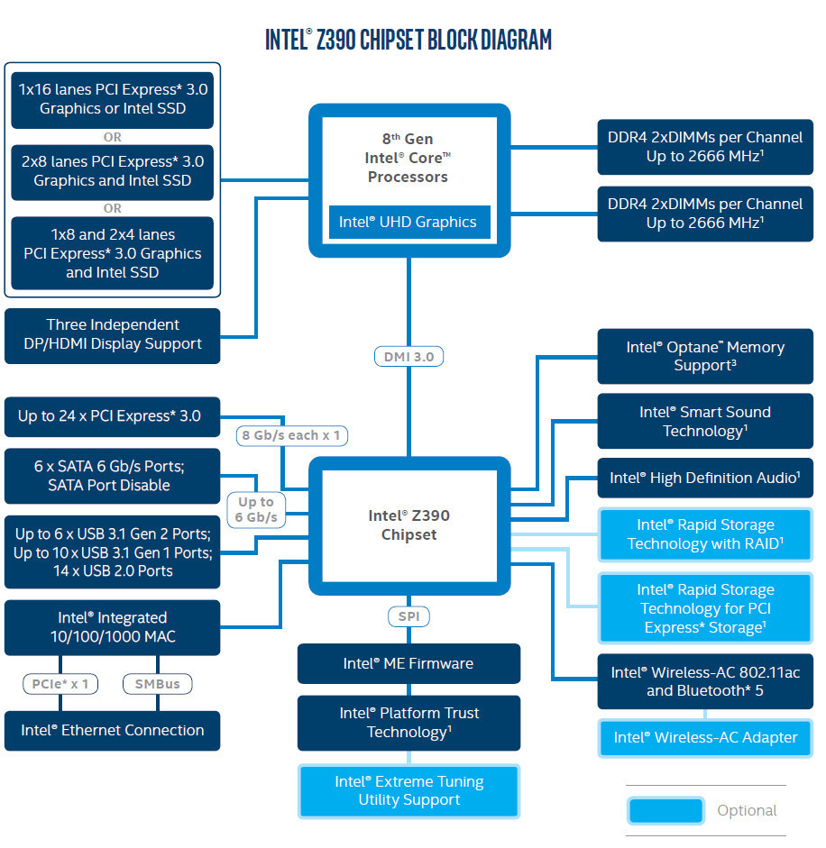
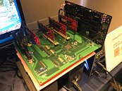
ASMedia Readies ASM2824 PCIe Switch Anticipating a Rise in M.2 Slots

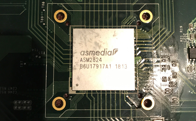
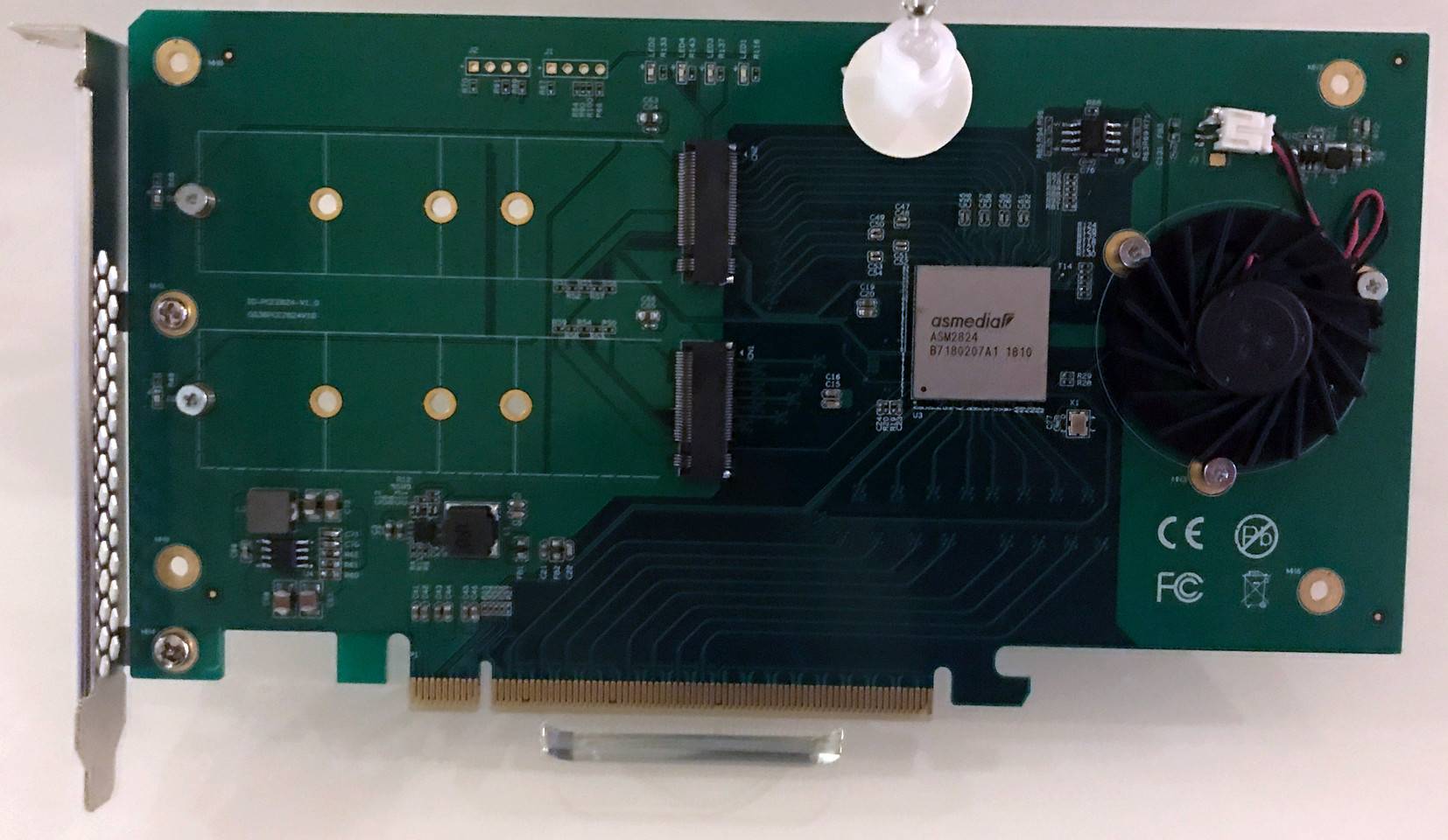
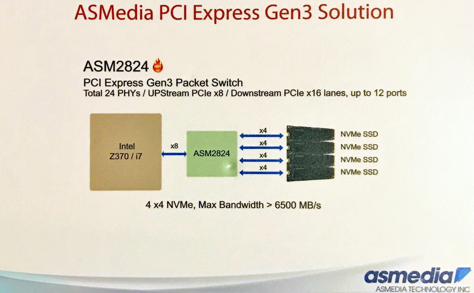
ASMedia is giving finishing touches to the ASM2824 PCI-Express gen 3.0 x24 switch. With half the fabric as the PLX PEX8747, the chip takes in PCI-Express 3.0 x8, and puts out four PCI-Express 3.0 x4 connections. In theory, this would let a motherboard designer create four M.2 PCIe 3.0 x4 slots from 8 downstream PCIe lanes of the Intel Z390 chipset, saving the remaining PCIe lanes for onboard USB 3.1 controllers (preferably sourced from ASMedia itself), since Intel canned the older 14 nm version of the Z390, which was supposed to put out six 10 Gbps USB 3.1 gen 2 and ten 5 Gbps USB 3.1 gen 1 ports directly from the PCH.

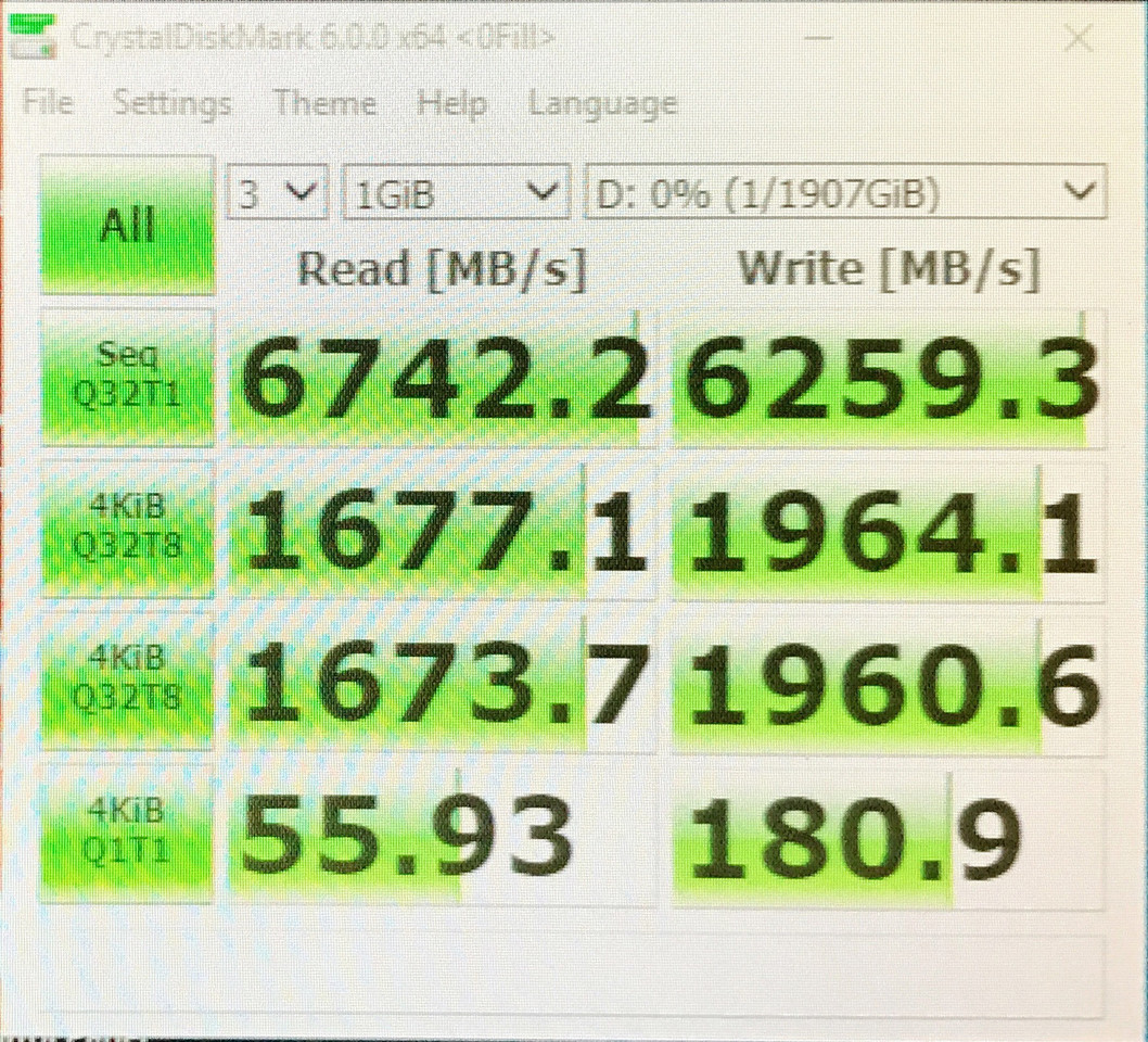
With all four downstream slots populated, ASMedia promises NVMe RAID bandwidths of up to 6,500 MB/s, with some CDM numbers even crossing 6,700 MB/s. Then again, one has to take into account that the test platform probably had the ASM2824 wired to the CPU's PCIe root-complex, and not that of the chipset. Intel is yet to modernize the lousy DMI 3.0 chipset-bus between its latest processors and chipset, and is physically PCI-Express 3.0 x4, which is fundamentally outdated for the bandwidth-heavy interfaces of this generation, such as USB 3.1, M.2 NVMe, and even the upcoming SD Express. The ASM2824 is also a godsend for the AMD AM4 platform, which not only has the same PCI-Express 3.0 x4 chipset bus between the AM4 SoC and the X470 chipset, but also a poor downstream PCIe feature-set of the X470, with just 8 gen 2.0 lanes. Motherboard designers can wire out all of those lanes to an ASM2824 for up to 24 downstream lanes.

Intel Z390 Platform, Intel Core i9 CPU Lineup Leaked?

According to a report from WCCFTech, Intel is prepping the release of the Z390 chipset and is gearing up to bring their Core i9 branding series to the mainstream desktop platforms. Apparently, Intel's renaming scheme serves as a way to add the required "branding impact" to the fact that the i9 series of processors is finally hitting the mainstream - but don't be deluded. As we've previously covered, Intel's Z390 chipset may well become a rebrand of sorts from the current Z370 chipset, after Intel found insufficient capacity at its 14 nm node (which has to cope with the vast majority of Intel silicon production, following the smattering of delays hitting its 10 nm process). Basically, Intel's Z390 chipset will bring forward features that weren't built on the Z370 chipset at its inception, but have since become part of Intel's lineup (read, for example, its H370 chipset): Intel Wireless-AC 802.11 AC and Bluetooth 5.0; Intel Wireless-AC Adapter; and up to 6 x USB 3.1 Gen 2 Ports.

According to WCCFTech, there's only confirmation of an 8-core, 16-thread CPU (Intel Core i9-9900K); a 6-core, 12-thread one (Intel Core i7-9700K) and a six-core, six-thread part (Intel Core i5-9600K ). No confirmation on an i3 part has been had yet, but it's very unlikely Intel has shelved that part of their lineup. A 4-core CPU is simply too important - from a yield perspective, mainly - for Intel to shelve it - and there's still enough demand for these, even with AMD's many-core democratization push.

Intel Shelves Z390 Express As We Knew It, Could Re-brand Z370 as Z390

Intel is rumored to have shelved the iteration of its upcoming Z390 Express chipset as earlier publicized, the one which had certain new hardware features. It could now re-brand the existing Z370 Express as Z390 Express and probably bolster its reference design with heftier CPU VRM specifications, to cope better with its upcoming 8-core LGA1151 processors. The Z370 Express is similar in feature-set to the brink of being identical to its predecessor, the Z270 Express. This move could impact certain new hardware features that were on the anvil, such as significantly more USB 3.1 gen 2/gen1 ports directly from the PCH, integrated WiFi MAC, and Intel SmartSound technology, which borrowed certain concepts from edge-computing to implement native speech-to-text conversion directly on the chipset, for improved voice control latency and reduced CPU overhead.

The reasons behind this move could be a combination of last-minute cost-benefit analyses by Intel's bean-counters, and having to mass-produce Z390 Express on the busier-than-expected 14 nm silicon fabrication node, as opposed to current 300-series chipsets being built on the 22 nm node that's nearing the end of its life-cycle. Intel probably needed the switch to 14 nm for the significant increases in transistor-counts arising from the additional USB controllers, the WiFi MAC, and the SmartSound logic. Intel probably doesn't have the vacant 14 nm node capacity needed to mass-produce the Z390 yet, as its transition to future processes such as 10 nm and 7 nm are still saddled with setbacks and delays; and redesigning the Z390 (as we knew it) on 22 nm may have emerged unfeasible (i.e. the chip may have ended up too big and/or too hot). The Z390 Express chipset block-diagram, which we published in our older article has been quietly removed from Intel's website. It's also rumored that this move could force AMD to rethink its plans to launch its Z490 socket AM4 chipset.

Intel Announces Core i7-8086K Limited Edition Six-core Processor

Intel today announced the Core i7-8086K six-core processor in the LGA1151(v2) package, compatible with 300-series chipset. This processor commemorates 40 years since the company's 8086 processor, which was the spiritual ancestor of the x86 architecture that dominates modern day computing. Based on the same 14 nm "Coffee Lake" silicon as the i7-8700K, this chip features high clock speeds of 4.00 GHz nominal, with a maximum Turbo Boost frequency of 5.00 GHz. Like the i7-8700K, it features 256 KB of dedicated L2 cache per core, and 12 MB of shared L3 cache. The processor will go on sale from 8th June, the company didn't reveal pricing, but it's rumored to be a conspicuous USD 486.

Intel Core i7-8086K Listed, First 5.00 GHz Processor

Intel is commemorating 40 years of its 8086 processor, the spiritual ancestor of the x86 machine architecture that rules modern computing, with a special edition socket LGA1151 processor, dubbed Core i7-8086K. The chip appears to feature a nominal clock speed of 4.00 GHz, with a maximum Turbo Boost frequency of 5.00 GHz, making it the first mainstream desktop processor from Intel to hit the 5.00 GHz mark, out of the box.

The Core i7-8086K is more likely to be based on a special bin of the 14 nm, 6-core/12-thread "Coffee Lake" silicon, rather than being something next-gen or 8-core. The retail SKU bears the part number "BX80684I78086K." The chip will be compatible with Intel 300-series chipset motherboards. Pre-launch listings put its price around $486, which is along expected lines, as it's 70-100 EUR pricier than the i7-8700K. Intel could unveil the Core i7-8086K at the 2018 Computex (specifically on the 8th of June), alongside the first motherboards based on its Z390 Express chipset.

AMD Readies Athlon 200GE and Athlon Pro 200GE: First Athlon Branded "Zen"

AMD is giving finishing touches to the Athlon 200GE (YD200GC6M2OFB) and Athlon Pro 200GE (YD200GC6M20FB) socket AM4 APUs, which will likely be a part of the company's answer to Intel's Pentium Gold series. The "E" brand extension denotes energy-efficiency, and both chips have a rated TDP of just 35W. The two are based on AMD's 14 nm "Raven Ridge" silicon, and pack a 2-core/4-thread CPU based on the "Zen" microarchitecture, clocked at 3.20 GHz.

Unlike previous few generations of Athlon-branded parts, which were essentially socket FM2(+) APUs devoid of integrated graphics, the Athlon 200GE and Athlon Pro 200GE do feature the Radeon Vega integrated graphics solution, but we expect it to be watered down compared to the Ryzen 2000G series chips. What sets the Athlon Pro part apart from its non-Pro sibling is the same feature that set Ryzen Pro apart, such as SEV. The two chips surfaced on the updated CPU compatibility lists of ASUS Crosshair VII Hero X470.

A Push for the Higher Margin: Intel Reportedly Discontinues Production of Its H310 Chipset

A report straight out of DigiTimes, citing industry sources, says that Intel has discontinued production of its H310 chipset. The decision has apparently stemmed from lower than expected production capacity for chipsets on the 14 nm process. When that happens, production focus must shift to a specific part: in this case, Intel obviously went with the option with the lower opportunity cost, and increased production of the Z370 chipset: the one with the increased feature-set, and, most likely than not, higher margins.

After a single month of tight supply for the H310 chipset, motherboard makers are now forced to use Intel's B360 chipset in their more cost-conscious options as well - a part which carries higher cost, and thus precludes manufacturers from hitting all the price points they usually would with a fully vertical Intel chipset lineup. Speculation has emerged claiming Intel suspended the supply of H310 because they have chosen to conduct a manufacturing process change from the tight-supply 14 nm (used across almost all of Intel's production stack, both consumer and enterprise) to a 22 nm fabrication technology. Further speculation places this constrained 14 nm supply as existent because of the delay in advancing to 10 nm, a process that Intel expected to be producing in volume by now (and since a while back, to be fair).

AMD Teases Its 7 nm Vega Instinct Accelerator - Data-Pushing Silicon Deployed

AMD has announced via its Twitter feed that the Vega die shrink from current 14 nm down to 7 nm has actually coalesced into a hardware product that can be tested and vetted at their labs. Via a teaser image, the company said that "7nm @RadeonInstinct product for machine learning is running in our labs."

Of course, working silicon is only half the battle - considerations such as yields, leakage, and others are all demons that must be worked out for actual production silicon, which may thus be some months off. Only AMD and TSMC themselves themselves know how the actual production run went - and the performance and power efficiency that can be expected from this design (remember that AMD's CEO Lisa SU herself said they'd partner with both TSMC and Globalfoundries for the 7 nm push, though it seems TSMC may be pulling ahead in that field). Considering AMD's timeline for the die-shrunk Vega to 7 nm - with predicted product launch for 2H 2018 - the fact that there is working silicon being sampled right now is definitely good news.

Intel Rumored to Commemorate 40th Anniversary of the 8086 with a Special Core i7 SKU?

Intel recently celebrated 20 years of the Pentium brand that made the company a household name, with a special Pentium 20th Anniversary Edition G3258 SKU. If rumors are to be believed, the company could do something similar with the upcoming 40th anniversary of its 8086 processor, the distant ancestor of today's x86 architecture. Some sources even suggest that the company could take advantage of its 8th generation Core product cycle to launch a "Core i7-8086K" SKU.

Pictures surfaced on social media of the said "i7-8086K" SKU in the flesh, complete with a part number "SR3QQ." Based on the same 14 nm "Coffee Lake" silicon as the i7-8700K, this chip has a nominal clock speed of 4.00 GHz, a maximum Turbo Boost frequency above 5.00 GHz, an unlocked multiplier, and 12 MB of shared L3 cache. Intel could choose June 8th (around the 2018 Computex and the actual anniversary of 8086), to launch the new SKU.

Intel Expands 8th Gen. Core Desktop Processor Family, Introduces New Chipsets

Intel today expanded its 8th generation Core desktop processor family, to include xx new models across its Core i7, Core i5, and Core i3 brand extensions. The company also introduced entry-level Pentium Gold and Celeron processors. The chips are based on the 14 nm "Coffee Lake" silicon, and are compatible with socket LGA1151 motherboards based on Intel 300-series chipset. Intel has relegated dual-core to the Celeron and Pentium Gold brands. The Celeron series includes 2-core/2-thread chips with 3 MB L3 cache; while the Pentium Gold series includes 2-core/4-thread chips with 4 MB L3 cache.

The company is launching the 8th generation Celeron series with two models, the G4900 and the G4920, clocked at 3.10 GHz, and 3.20 GHz, respectively. The Pentium Gold family has three parts, the G5400, the G5500, and the G5600, clocked at 3.70 GHz, 3.80 GHz, and 3.90 GHz, respectively. The 8th generation Core i3 family of 4-core/4-thread parts receives a new member, the i3-8300. Endowed with 8 MB of L3 cache, this chip is clocked at 3.70 GHz, and sits between the i3-8100 and the i3-8350K, but lacks the unlocked multiplier of the latter.

Intel Ships Industry's First 58G PAM4-Capable FPGA

Intel today announced it has begun shipping its Intel Stratix 10 TX FPGAs, the industry's only field programmable gate array (FPGA) with 58G PAM4 transceiver technology. By integrating the FPGA with 58G PAM4 technology, Intel Stratix 10 TX FPGAs can double the transceiver bandwidth performance when compared to traditional solutions. This exceptional bandwidth performance makes the Intel Stratix 10 TX FPGAs the essential connectivity solution for next-generation use cases: optical transport networks, network function virtualization (NFV), enterprise networking, cloud service providers and 5G networks applications where high bandwidth is paramount.

To facilitate the future of networking, NFV and optical transport solutions, Intel Stratix 10 TX FPGAs provide up to 144 transceiver lanes with serial data rates of 1 to 58 Gbps. This combination delivers a higher aggregate bandwidth than any current FPGA, enabling architects to scale to 100G, 200G and 400G delivery speeds. By supporting dual-mode modulation, 58G PAM4 and 30G NRZ, new infrastructure can reach 58G data rates while staying backward-compatible with existing network infrastructure. A wide range of hardened intellectual property (IP) cores, including 100GE MAC and FEC, deliver optimized performance, latency and power.

Intel Intros Core i3-8130U Dual-core Low-power Processor

Intel today introduced the Core i3-8130U dual-core (2-core/4-thread) ultra low-power processor for thin and light notebooks, and 2-in-1 convertibles. Based on the 14 nm "Kaby Lake-U" silicon, the chip features a TDP of just 15W, making it ideal for all-day power devices. It is clocked at 2.40 GHz, with 3.40 GHz Turbo Boost frequency, and packs 4 MB of L3 cache. In its TDP-down mode, the CPU idles at 800 MHz, lowering the TDP to 10W. Its dual-channel DDR4 memory controller supports up to 32 GB of DDR4-2400 or LPDDR3-2133 memory. On the display side of things are the UHD Graphics 620 iGPU with clock speed ranging between 300 MHz and 1.00 GHz, 24 execution units, and hardware-acceleration for H.265/HEVC with 10bpc color.

AMD Officially but Silently Downgrades Radeon RX 560 with an 896 SP Variant

The phenomenon of Radeon RX 560 graphics cards with 896 stream processors is more widespread than earlier thought. It looks like RX 560 cards with 896 stream processors will be more widely available than the previously thought Greater China region; with AMD silently editing the specifications of the SKU to have either 896 or 1,024 stream processors, as opposed to the 1,024 it originally launched with. There are no clear labeling guidelines or SKU names to distinguish cards with 896 stream processors from those with 1,024.

The Radeon RX 560 and the previous-generation RX 460 are based on the 14 nm "Polaris 11" silicon, which physically features 16 GCN compute units (CUs), each packed with 64 stream processors. The RX 560 originally maxed this silicon out, with all 16 CUs being enabled, while the RX 460 has two CUs locked. The decision to change specs of the RX 560 effectively makes it a re-brand of the RX 460, which is slower, and provides fertile grounds for bait-and-switch lawsuits.

Intel Announces "Coffee Lake" + AMD "Vega" Multi-chip Modules

Rumors of the unthinkable silicon collaboration between Intel and AMD are true, as Intel announced its first multi-chip module (MCM), which combines a 14 nm Core "Coffee Lake-H" CPU die, with a specialized 14 nm GPU die by AMD, based on the "Vega" architecture. This GPU die has its own HBM2 memory stack over a 1024-bit wide memory bus. Unlike on the AMD "Vega 10" and "Fiji" MCMs, in which a silicon interposer is used to connect the GPU die to the memory stacks, Intel deployed the Embedded Multi-Die Interconnect Bridge (EMIB), a high-density substrate-level wiring. The CPU and GPU dies talk to each other over PCI-Express gen 3.0, wired through the package substrate.

This multi-chip module, with a tiny Z-height, significantly reduces the board footprint of the CPU + discrete graphics implementation, when compared to having separate CPU and GPU packages with the GPU having discrete GDDR memory chips, and enables a new breed of ultra portable notebooks that pack a solid graphics muscle. The MCM should enable devices as thin as 11 mm. The specifications of the CPU and dGPU dies remain under the wraps. The first devices with these MCMs will launch by Q1 2018.
A video presentation follows.

AMD "Raven Ridge" Silicon Detailed

The "Zen" CPU micro-architecture seems to be turning AMD's fortunes as it reported its first black quarter in years. The 14 nm "Zeppelin" or "Summit Ridge" die is at the heart of this change. This 8-core CPU die is implemented on everything from performance mobile packages, to single-die mainstream-desktop socket AM4 under the Ryzen 3, Ryzen 5, and Ryzen 7-series, 2-die high-end desktop (HEDT) multi-chip modules under Ryzen Threadripper, and the 4-die enterprise multi-chip modules under the EPYC brand. The next logical step for AMD with its new "Zen" CPU IP was to fuse it with the "Vega" graphics architecture, and give its APU lineup a much needed overhaul. At the heart of this move is the new 14 nm "Raven Ridge" silicon.

While "Summit Ridge" is the combination of two "Zen" CCX (quad-core CPU complex) units making up an 8-core CPU die that lacks integrated graphics, the "Raven Ridge" silicon combines one "Zen" CCX with an integrated graphics core based on the "Vega" architecture. AMD's new Infinity Fabric interconnect ferries data between the CCX and the iGPU, and not an internal PCIe link. The CCX houses four "Zen" CPU cores with 64 KB of L1I cache, 32 KB of L1D cache, 512 KB of dedicated L2 cache, and 4 MB of L3 cache shared between the four cores.

Intel Introduces Neuromorphic Self-Learning Chip Codenamed "Loihi"

Intel has been steadily increasing its portfolio of products in the AI space, through the acquisition of multiple AI-focused companies such as Nervana, Mobileye, and others. Through its increased portfolio of AI-related IP, the company is looking to carve itself a slice of the AI computing market, and this sometimes means thinking inside the box more than outside of it. It really doesn't matter the amount of cores and threads you can put on your HEDT system: the human brain's wetware is still one of the most impressive computation machines known to man.

That idea is what's behind of neuromorphic computing, where chips are being designed to mimic the overall architecture of the human brain, with neurons, synapses and all. It marries the fields of biology, physics, mathematics, computer science, and electronic engineering to design artificial neural systems, mimicking the morphology of individual neurons, circuits, applications, and overall architectures. This, in turn, affects how information is represented, influences robustness to damage due to the distribution of workload through a "many cores" design, incorporates learning and development, adapts to local change (plasticity), and facilitates evolutionary change.

Intel Announces Availability of Core i9-7980XE and Core i9-7960X

Intel expanded the upper end of its Core X "Skylake-X" HEDT processor family, with the introduction of the Core i9-7980XE 18-core flagship processor, and the i9-7960X 16-core processor. Designed to give pro-sumers and PC enthusiasts extreme mega-tasking performance, the i9-7980XE features all components physically present on the 14 nm "Skylake-X" silicon, featuring 18 cores, with HyperThreading enabling 36 threads; 1 MB of dedicated L2 cache per core, 24.75 MB of shared L3 cache, and rather restrained clock speeds of 2.60 GHz, with Turbo Boost speeds of 4.20 GHz, and Turbo Boost Max 3.0 frequency of 4.40 GHz.

Despite its gargantuan core-count, the TDP of this chip is rated at 165W, lower than the 180W rated for competing Ryzen Threadripper processors. The other high-end processor launched by Intel is the Core i9-7960X. This 16-core/32-thread chip features clock speeds of 2.80 GHz, with 4.20 GHz Turbo Boost, and 4.40 GHz Turbo Boost Max 3.0. It features 22 MB of shared L3 cache, and 1 MB of dedicated L2 cache per core. The Core i9-7980XE is priced at USD $1,999 in the retail channel; while the Core i9-7960X goes for $1,699.

Intel 8-core LGA1151 Processor will be 14 nm "Coffee Lake" Based

The 8-core processor Intel is planning to launch in the second half of 2018 will be based on the current 14 nanometer "Coffee Lake" micro-architecture, according to leaked XTU errata log. A curious looking change-log entry reads "[CFL] Added support for 8,2 core," where "CFL" is the three-letter contraction of "Coffee Lake," just as "KBL" stands for "Kaby Lake" and "HSW" for "Haswell."

This hints at the two directions in which Intel is expanding its 8th generation mainstream desktop lineup. On the upper-end of the spectrum, one can expect the augmentation of 8-core/16-thread parts, while at the lower end, one can expect dual-core parts, likely branded under the Pentium and Celeron brands. Intel's MSDT lineup will be led by 6-core parts under the Core i5 and Core i7 extensions, and quad-core parts under the Core i3 extension; with 6-core/12-thread Core i7 SKUs leading the pack till the second-half of 2018.

Intel Intros Core i9-7920X HEDT Processor

Intel today announced availability of its Core i9-7920X high-end desktop (HEDT) processor in the LGA2066 package, designed for motherboards based on the Intel X299 Express chipset. The chip is priced at USD $1,199 in the retail market, a $200 premium over its previous flagship part, the i9-7900X. The new i9-7920X is a 12-core/24-thread processor based on 14 nm "Skylake-X" silicon, and has a rated TDP of 140W.

The Core i9-7920X features a nominal clock speed of 2.90 GHz, with a maximum Turbo Boost frequency of 4.30 GHz, and Turbo Boost Max 3.0 frequency of 4.40 GHz. It features 1 MB of dedicated L2 cache per core, and 16.50 MB of shared L3 cache. The chip features the full 44-lane PCI-Express gen 3.0 root complex available on the silicon, and its quad-channel DDR4 integrated memory interface, supporting up to 128 GB of memory.

AMD RX Vega Supply Issues to Persist At Least Until October - Digitimes

DigiTimes is reporting, through "sources from the upstream supply chain", that AMD's current shortage of RX Vega cards to distribute to the retail market will continue at least until October. The tech reporting site says that sources are pointing towards the package integration of HBM2 memory (from SK Hynix or Samsung Electronics) and the Vega GPU (manufactured on Global Foundries' 14 nm FinFet) as being at fault here, due to low yield rates for this packaging effort. However, some other sources point towards the issue being with the packaging process itself, done by Advanced Semiconductor Engineering (ASE) through use of SiP technology. Whichever one of these cases may be, it seems the problem lies with AMD's choice to use HBM2 on their Vega graphics architecture.

As a footnote to its story, DigiTimes is also reporting that according to industry sources, NVIDIA has, in light of RX Vega's performance, decided to postpone the launch of Volta-based GPUs towards the first quarter of 2018.

Intel 8th Gen Core i5 and Core i7 Retail Boxes Pictured

Here are the first pictures of the retail boxes of 8th generation Intel Core i5 and Core i7 processors. The first wave of processors based on Intel's new 14 nm "Coffee Lake" silicon will be 6-core parts in the Core i5 and Core i7 brands, which will be launched on 22 August; with Core i3 following on much later in the year, or even early-2018. The boxes confirm several things about these chips, beginning with the fact that their integrated graphics cores will be branded "Intel UHD Graphics 6xx," and that they will require motherboards based on Intel 300-series chipset, even though their socket is "LGA1151."

There doesn't appear to be a socket key difference between these processors and "Kaby Lake," so it's possible that while 300-series chipset motherboards support older "Kaby Lake" and "Skylake" processors, "Coffee Lake" will only work on 300-series chipset, and not older 200-series or 100-series. Intel making the bold move of branding its new integrated graphics "UHD" could hint at its credentials with hardware-accelerated decoding of new video formats such as 10-bit VP9 at 4K without breaking a sweat; and new display connector standards such as HDMI 2.0 and DP 1.4. The various models that make up the first wave of 8th generation Core i5 and Core i7 desktop processors, are tabled below.

Intel Core i3-8300 Detailed - First Quad-Core i3

Intel Core i3-8300 could be the company's first quad-core processor to bear the Core i3 badge. Based on the 14 nm "Coffee Lake-S" silicon, This SKU could be priced in the upper-band of the Core i3 lineup (around the USD $150 mark), offering four cores. As if that isn't surprising enough, this quad-core chip even reportedly features HyperThreading, enabling 8 logical CPUs for the OS to deal with.

For the first time, a Core i3 part will have more logical CPUs than a Core i5 part, which lacks HyperThreading. Such a feature disparity won't be new, as current Core i3 dual-core SKUs feature HyperThreading, which Core i5 quad-core parts lack. The i3-8300, however, will lack Turbo Boost, which Core i5 SKUs will feature. The chip reportedly features a clock speed of 4.00 GHz. The L3 cache amount and TDP of this chip remain unknown at this point. Intel could launch Core i3 "Coffee Lake" processors only by late-2017 or early-2018.

AMD X399 Platform Lacks NVMe RAID Booting Support

AMD's connectivity-rich Ryzen Threadripper HEDT platform may have an Achilles's heel after all, with reports emerging that it lacks support for booting from NVMe RAID. You can still have bootable NVMe RAID volumes using NVMe RAID HBAs installed as PCI-Express add-on cards. Threadripper processors feature 64-lane PCI-Express gen 3.0 root complexes, which allow you to run at least two graphics cards at full x16 bandwidth, and drop in other bandwidth-hungry devices such as multiple PCI-Express NVMe SSDs. Unfortunately for those planning on striping multiple NVMe SSDs in RAID; the platform lacks NVMe RAID booting support. You should still be able to build soft-RAID arrays striping multiple NVMe SSDs, just not boot from them. Pro-sumers will still be able to dump their heavy data-sets onto such soft-arrays. This limitation is probably due to PCI-Express lanes emerging from different dies on the Threadripper MCM, which could present problems to the system BIOS to boot from.

Ryzen Threadripper is a multi-chip module (MCM) of two 8-core "Summit Ridge" dies. Each 14 nm "Summit Ridge" die features 32 PCI-Express lanes. On a socket AM4 machine, 4 of those 32 lanes are used as chipset-bus, leaving 28 for the rest of the machine. 16 of those head to up to two PEG (PCI-Express Graphics) ports (either one x16 or two x8 slots); and the remaining 12 lanes are spread among M.2 slots, and other onboard devices. On a Threadripper MCM, one of the two "Summit Ridge" dies has chipset-bus access; 16 lanes from each die head to PEG (a total of four PEG ports, either as two x16 or four x8 slots); while the remaining are general purpose; driving high-bandwidth devices such as USB 3.1 controllers, 10 GbE interfaces, and several M.2 and U.2 ports.

AMD Ryzen Threadripper TDP and Cache Sizes Confirmed

AMD maybe have shaken up the HEDT (high-end desktop) processor market with three Ryzen Threadripper SKU announcements early this week; but the two specifications that eluded us were their rated TDP and cache amounts. The first Ryzen Threadripper models will be available in the market from the 10th of August, and will include the 12-core/24-thread 1920X and the flagship 16-core/32-thread 1950X. Both models will feature the full 32 MB of L3 cache available from a pair of 14 nm "Summit Ridge" dies, which work out to "total cache" (L2+L3) amounts of 38 MB for the 1920X and 40 MB for the 1950X. The TDP of the 1920X and 1950X is rated at 180W. The TDP and cache configuration of the 8-core/16-thread 1900X remains unknown, for now.

It's Coffee Lake Again: Intel Six-Core Processor Surfaces on Geekbench

After rearing its head on SiSoft Sandra, it seems that an engineering sample of Intel's upcoming Coffee Lake CPUs has appeared again - this time on Geekbench. Coffee Lake is supposed to be Intel's version of a core-count democratization. It is expected that the company will introduce six-core CPUs to their i7 line of processors (since apparently the i9 moniker is now limited to the company's HEDT solutions). This should bring about a reshuffle of Intel's CPU line-up, though it remains to be seen how the company will go about that way.

Moving on to the actual Geekbench scores, Intel's 6-core, 12-thread CPU delivers a 4,619 single-core score, and a 20,828 multi-core score. This is more or less inline with AMD's Ryzen 5 1600X 6-core, 12-thread processor. However, AMD's solution is clocked higher than this particular engineering sample was (3.6 GHz on the Ryzen 5 vs 3.2 GHz on the Intel Coffee Lake sample, a 400 MHz difference.) This probably means that finalized Intel silicon with come with higher clocks, and therefore, a more commanding performance.
Return to Keyword Browsing
Apr 26th, 2024 07:39 EDT change timezone

New Forum Posts

Popular Reviews

Controversial News Posts