News Posts matching #Intel 18A

Return to Keyword Browsing

Intel 18A-P Node Delivers 9% Performance Increase, 18% Power Savings

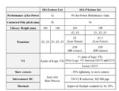
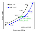
Intel's next-generation 18A node is ready, and the company has tested it, showcasing some impressive results. At the VLSI 2026 Symposium in Honolulu, Hawaii, Intel will present its new research on the capabilities of the upcoming 18A-P node. According to the paper, the 18A-P node can deliver a 9% performance increase at the same power level or achieve 18% power savings at the same performance level compared to the standard 18A. However, there is more to this than meets the eye. Typically, node generations show similar performance and power improvements across generations. What would be expected in terms of power and performance improvements when transitioning from 18A to 14A is now already available with the 18A-P node, but without any density improvements. This makes the 18A-P node a very attractive option for external customers who expect the transistor density of the 18A node found in "Panther Lake," but with significantly better characteristics.

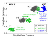
For reference designs, Intel uses an Arm core sub-block to test frequency and power scaling. The new 18A-P node can yield much better results on paper, but one of the most interesting improvements is in manufacturing, specifically in something called skew corners. When a node is manufactured, no two transistors are identical due to the inherent physics of the manufacturing process, especially at today's scale. These variations are measured between fast and slow "corners," meaning faster and slower transistors. The skew refers to how wide the performance and power gap is between these transistors. Intel has managed to improve the skew corners on the 18A-P node by 30% compared to the standard 18A, meaning that power and performance characteristics are now more predictable, especially for parametric yields. This means that chip functions are now more predictable, and Intel has to deal with far fewer variations with the new node.

Below is Intel's paper abstract about the 18A-P node.

Intel Foundry Improves Yields Across Intel 4, Intel 3, and 18A Nodes

Intel posted strong Q1 2026 earnings results, indicating improvements across multiple verticals, from Intel Products to Intel Foundry divisions. Both groups experienced operational enhancements, but Intel Foundry achieved a significant milestone: yield improvement across all major foundry nodes currently in high-volume manufacturing. This includes Intel 4, Intel 3, and 18A nodes, which power the majority of Intel's product portfolio. In the latest Q1 2026 earnings call, Intel CFO David Zinsner noted that the company continues to improve yields on its older nodes, such as Intel 4 and Intel 3, while refining the yield of the current top-performing 18A node to reduce waste and increase the number of functional chips, even in larger dies.
David Zinsner, Intel CFOIntel Foundry operating loss in Q1 was $2.4 billion, improved $72 million quarter-over-quarter as better yields across Intel 4, Intel 3, and 18A drove higher gross margins. This was mostly offset by increased operating expenses associated with an intentional step-up in Intel 14A investments to support both internal and external customer evaluations. As a reminder, Intel Foundry carries the bulk of the cost associated with the early ramp of Intel 18A, and we expect Intel Foundry's operating loss to improve through the year as 18A continues to ramp into volume and yields improve further. Within the quarter, Intel Foundry delivered output above our expectations, drove steady improvements in yields, and met key 14A milestones.

Intel Posts Strong Q1 2026 Results, Lands Tesla as First 14A Node Major Customer

Intel has posted better-than-expected Q1 2026 results, with $13.58 billion in revenue, up 7.2% year over year and well ahead of the $12.42 billion analysts had forecast. Adjusted earnings per share hit 29 cents against an expectation of just one cent, sending the stock up more than 15% in after-hours trading. Data center and AI were strong performers, bringing in $5.1 billion against estimates of $4.41 billion. The foundry division revenue generated $5.4 billion, though the vast majority of that was Intel's own internal business. External customer revenue was less than $200 million, mostly legacy wafer work. Also, Intel ASIC business is on track for more than $1 billion in revenue this year. Part of the Q1 surprising results came from Intel clearing out finished goods inventory it hadn't expected to move, according to CFO David Zinsner. The company is also raising chip prices to offset rising production costs, which is reflected in its Q2 guidance of $13.8 to $14.8 billion, a bit more than the $13 billion Wall Street had estimated.

Going back to the foundry side, Intel scored two notable wins on this front. Tesla signed on as Intel's first major 14A customer for Elon Musk's Terafab AI chip complex in Austin, however, the details of this deal are still unknown. The most logical scenario is that Terafab will license the Intel 14A process, but neither side has confirmed it. The second win came earlier this month when Intel expanded its AI CPU deal with Google, the two companies extending their co-development of custom ASIC-based IPUs.

Intel Intros Core Ultra Series 3 vPro "Panther Lake" Processors for Commercial Notebooks

Intel today announced its ambitious Core Ultra Series 3 vPro "Panther Lake" mobile processors for commercial notebooks. The processors build on the Core Ultra Series 3 processors launched in the consumer segment earlier this year, bolstering them with the entire Intel vPro platform for remote manageability and enhanced enterprise security. The new "Panther Lake" microarchitecture debuts the Intel 18A foundry-node, a must-win foundry note for Intel that offers superior transistor density, energy efficiency, and clock speeds compared to the TSMC N3 foundry node on which Intel built its previous Core Ultra 200V "Lunar Lake" and Core Ultra Series 2 "Arrow Lake" mobile processors.

The new "Panther Lake" architecture introduces the new "Cougar Cove" P-core that's optimized for Intel 18A node with enhancements to its branch predictor, memory disambiguation, and TLB improvements to provide a minor IPC increase over the previous "Lion Cove" P-core. The new "Darkmont" E-core further pushes up IPC over the previous "Skymont." Intel Thread Director sees further improvements for more accurate scheduling. The processors launching today come with the entire constellation of Intel vPro manageability features, including Device Discovery, Innovation Platform Framework, Unique Platform ID, total memory encryption with multi-key, Stable IT Platform, Intel AMT, platform service record, remote erase, one-click recovery, and CET. Security features include Intel TXT, platform trust technology, VT with redirect protection, Boot Guard, BIOS Guard, partner security engine, linear address-space separation, and Intel Threat Detection technology.

Intel Core Ultra Series 3 "Panther Lake-H" Die Annotated

Intel's recently announced Core Ultra Series 3 "Panther Lake-H" mobile processor die-shot has been annotated by Kurnal Insights. "Panther Lake-H" is a disaggregated processor, just like its predecessor, "Arrow Lake-H," and "Meteor Lake," but Intel has followed a disaggregation plan resembling that of "Lunar Lake," where an SoC tile contains the CPU cores across both the main compute complex and low-power island; the NPU, and the processor's main integrated memory controllers; the Graphics tile contains the iGPU's number-crunching machinery, the Xe cores; while the I/O tile contains the chip's various platform I/O components.

The SoC tile is built on the Intel 18A foundry node. On the mainstream notebook "Panther Lake-H" processor variants, such as the one annotated below, the Graphics tile contains 4 Xe cores, and is built on the Intel 3 foundry node. On the ultraportable "Panther Lake-U" processor with powerful integrated graphics meant for devices lacking discrete GPUs, the Graphics tile has 12 Xe cores, and is built on the TSMC N3E node. The I/O tile continues to be built on the same TSMC N6 node as the ones on previous-generation "Arrow Lake" processors.

Intel Launches Xeon 6+ "Clearwater Forest" Xeon with 288 E-Cores on 18A Process

Intel used its MWC conference in Barcelona to showcase its most core-dense Xeon 6+ processor, codenamed "Clearwater Forest." As one of Intel's most complex chiplet designs, the package combines 12 compute chiplets manufactured on an Intel 18A node with three active base tiles on Intel 3 and two I/O tiles on Intel 7. In this configuration, each compute tile contains six modules of four "Darkmont" efficiency cores, providing 24 E-cores per tile and a maximum of 288 "Darkmont" E-cores on a single socket. A two-socket system, therefore, approaches 576 cores. The design connects clusters with a high-bandwidth on-chip fabric and stacks die using Foveros Direct 3D, while EMIB links connect multiple tiles in a 2.5D arrangement.

Each "Darkmont" E-core comes with a 64 KB instruction cache, a wider front end, and a larger out-of-order window to sustain more in-flight work. Execution resources and the number of execution ports have been increased to improve parallel integer and vector throughput. Physically, clusters are grouped in four-core units sharing about 4 MB of L2 cache per group, and the package-level last-level cache can exceed a gigabyte, with about 1,152 MB of combined last-level cache across the package. "Clearwater Forest" supports the existing Xeon server platform socket, 12 memory channels, and broad I/O, including 96 PCIe 5.0 lanes and 64 CXL 2.0 lanes. Memory speed targets push toward DDR5-8000.

NVIDIA to Build GPUs on Intel Foundry from 2028: Report

NVIDIA's upcoming "Feynman" AI GPU will partially use Intel Foundry nodes, a DigiTimes report says. NVIDIA recently invested a 5% stake in Intel, and is exploring tapping into Intel Foundry manufacturing capacity. In particular, NVIDIA is interested in the Intel 18A and 14A foundry nodes for certain components of its upcoming "Feynman" AI GPU that launches in 2028, succeeding the current "Rubin" AI GPU. NVIDIA also intends to tap into Intel's EMIB technology for its chiplet interconnectivity, the report says.

The "Feynman" AI GPU will still be majorly TSMC-based, with its core IP being built on die(s) leveraging TSMC A16 (1.6 nm) foundry node, which is expected to make up 75% of the chip's value. The remaining silicon content will be built on Intel 18A or Intel 14A nodes, and the chip's final packaging is expected to take place in U.S. soil, at Intel Foundry. This way, it will be Intel handling the EMIB chiplet bonding. "Feynman" is expected to implement a newer memory standard, such as HBM4e or even HBM5, and significantly increase memory per package, so each chip can handle trillion-parameter scale models.

Intel Reports Q4 and Full-Year 2025 Financial Results, Shares Down 11%

Intel Corporation today reported fourth-quarter and full-year 2025 financial results. "Our conviction in the essential role of CPUs in the AI era continues to grow," said Lip-Bu Tan, Intel CEO. "We delivered a solid finish to the year and made progress on our journey to build a new Intel. The introduction of our first products on Intel 18A - the most advanced process technology developed and manufactured in the United States - marks an important milestone, and we're working aggressively to grow supply to meet strong customer demand. Our priorities are clear: sharpen execution, reinvigorate engineering excellence, and fully capitalize on the vast opportunity AI presents across all of our businesses."

"We exceeded Q4 expectations across revenue, gross margin, and EPS even as we navigated industry-wide supply shortages," said David Zinsner, Intel CFO. "We expect our available supply to be at its lowest level in Q1 before improving in Q2 and beyond. Demand fundamentals across our core markets remain healthy as the rapid adoption of AI reinforces the importance of the x86 ecosystem as the world's most widely deployed high-performance compute architecture."

Intel Launches Core Ultra Series 3 "Panther Lake" Mobile Processors on Intel 18A Node

Today at CES, Intel unveiled Intel Core Ultra Series 3 processors, the first AI PC platform built on Intel 18A process technology that was designed and manufactured in the United States. Powering over 200 designs from leading, global partners, Series 3 will be the most broadly adopted and globally available AI PC platform Intel has ever delivered.

Within the Intel Core Ultra Series 3 mobile lineup, a new class of Intel Core Ultra X9 and X7 processors come packed with the highest performing, integrated Intel Arc graphics. They are purpose-built for multitaskers that handle advanced workloads like gaming, creation and productivity on the go. The top SKUs feature up to 16 CPU cores, 12 Xe -cores and 50 NPU TOPS, delivering up to 60% better multithread performance over 77% faster gaming performance and up to 27 hours of battery life.

NVIDIA Tested Intel's 18A Node but Did Not Commit to Intel Foundry

According to a report from Reuters, NVIDIA has explored using Intel Foundry's 18A node but has not proceeded to mass production. Reuters states, "NVIDIA recently tested out whether it would manufacture its chips using Intel's production process known as 18A but stopped moving forward, two people familiar with the matter said. NVIDIA did not answer a request for comment." This is not necessarily a negative sign for Intel Foundry, as many customers have previously approached Intel to try out the 18A node. It is common for chip designers to evaluate what TSMC's competitors offer before committing to additional foundry capacity.

For the 18A node, the general impression is that it primarily serves Intel's internal products. Future versions, like 18A-P and 18A-PT, aim to attract external customers and are expected to be long-term Intel Foundry products. Intel's 14A node is becoming a critical product for Intel Foundry, with active development targeting a 2027 release. As Intel collaborates with customers on the node design, potential foundry partners are assessing whether the upcoming technology meets their needs. Early customer feedback indicates strong satisfaction with the development progress, with those familiar with the node describing it as genuinely competitive.

Intel's Fab 52 is Bigger Than TSMC Arizona, Produces More Than 40,000 Wafers Per Month

Intel Foundry has massive capacity in the United States, with its size surpassing that of TSMC's Arizona campus in terms of production capacity and building space. A CNBC crew visited Intel's Fab 52 in Arizona to explore its operations, uncovering some intriguing details about wafer capacity and future production plans. According to their report, Intel's Fab 52 produces approximately 10,000 wafers per week, totaling over 40,000 wafers per month. These wafers are manufactured using the 18A node, Intel's most advanced design, featuring innovations such as a backside power delivery network and gate-all-around transistors, among others.

Compared to TSMC's facility in Arizona, Intel's manufacturing capacity and node designs are superior. TSMC currently produces about 20,000 wafers per month at the older N5 and N4 nodes, which are 5 nm class, in the Fab 21 Phase 1 stage. Although TSMC plans to expand Fab 21 to increase wafer capacity and introduce more advanced nodes, these advancements will primarily remain in Taiwan, keeping U.S.-based TSMC production a few generations behind. Intel, on the other hand, has a limited number of external partners using its nodes, with the 18A node being primarily for Intel's own products, including the upcoming "Panther Lake" processor, and some future generations.

European E-tailers Start Listing "Panther Lake" Chip-powered MSI Laptops

MSI seems to be leading the Intel "Panther Lake" mobile processor charge, as demonstrated by the company's November showcasing of sleek next-gen Prestige laptops/notebooks. Weeks later, preliminary retail listings have started popping up in Western Europe, indicating an imminent release of first batch hardware. Intel and its manufacturing partners are expected to fully unveil "Core Ultra 300 series" APU-based devices at CES 2026, but various pre-event leaks have already produced major spoilers. The ever watchful momomo_us has sniffed out unreleased MSI SKUs, bearing identifiers that could be associated with the brand's Prestige product line. Sitting atop the leaked stack, is a potential flagship 16-inch model (16i)—basic specifications include a 2.8K 120 Hz OLED display, 32 GB LPDDR5X of system memory, and a 2 TB SSD.

Crucially, Team Blue's rumored "Panther Lake-H" headliner—the 16-core Core Ultra X9 388H—is identified as this device's processor of choice. Likely placeholder pricing is in effect here, since the top-level MSI model bears a €3000+ (including VAT) tag. Two other SKUs seemingly make use of Intel's next-gen "4+8+4" core configured designs: powered by Core Ultra 386H and Core Ultra X7 358H processors. The cheapest option sports a Core Ultra 355 (non-H) unit, occupying the stack's budget-oriented "4+0+4" lineup. In addition, further sleuthing produced evidence of Walmart listing a not-yet-launched 16-inch HP OmniBook X Flip model—at $999—also based around Team Blue's forthcoming 8-core Core Ultra 355 mobile chip.

Intel Claims "Lunar Lake" and "Arrow Lake" Demand Outpaces Wafer Supply

Intel was presenting at 2025 UBS Global Technology and AI Conference, revealing interesting details about the demand for its "Lunar Lake" and "Arrow Lake" processors. On the question from one of the analysts that some assume Intel isn't selling its new products and there is no demand, Intel's John Pitzer answered "Quite frankly, if we had more Granite wafers, we'd be selling more Granite. If we had more Lunar Lake wafers, we'd be selling more Lunar Lake. If we had more Arrow Lake wafers, we'd be selling more Arrow Lake. And so I think we feel pretty good about where we are in the AI PC transition. And we feel very good about where we are in the initial phase of the Granite ramp, which is our latest generation server part."

This puts an end to the speculation that Intel's products aren't selling well, and the recent Q3 revenue figure of $13.7 billion matches that. Additionally, Intel made comments about its internal and external manufacturing capacity. Intel's "Lunar Lake" and "Arrow Lake" are SoCs that are fully outsourced to TSMC, with Intel performing the packaging. Hence, Intel's limited capacity booked at TSMC is not enough to satisfy the demand. However, starting with "Panther Lake," the wafer supply is getting back in-house as 18A yields mature. All the "Panther Lake" logic dies will be manufactured in-house, compared to 0% of logic dies manufactured in-house for "Arrow Lake" and "Lunar Lake."

Intel Could Manufacture Apple M-Series Chips in 2027 with 18A-P Node

According to one of the analysts closest to the Apple supply chain, Ming-Chi Kuo, Intel is expected to manufacture Apple's advanced M-series of chips by 2027. According to Kuo, Apple has used version 0.9.1 of process design kit (PDK) designed for Intel 18AP node. With performance, density, power, and every other metric going according to plan, Intel could become Apple's source of advanced node production in 2027. Additionally, Apple is reportedly waiting for Intel to release 18AP PDK version 1.0 or 1.1, which is scheduled for Q1 of 2026. When that gets released, Apple will start with lowest-end M-series chip, used by MacBook Air and iPad Pro devices.

Interestingly, Intel expected customers to adopt more of the refined 18A nodes—like 18A-P and 18A-PT—and later 14A nodes, than its current vanilla 18A. The 18A-P node enhances Intel's 18A by incorporating RibbonFET and PowerVia technologies, which offer better performance and energy efficiency. Compared to the regular 18A node, these improvements include newly designed low-threshold voltage components, optimized elements to reduce leakage, and refined ribbon width specifications, all aimed at boosting performance-per-watt metrics. Apple's designs are very similar to Intel's "Lunar Lake," which includes compute and memory on a single package. This is made using the "Foveros" advanced packaging, which we covered here.
Intel-made Apple SoC

GMKtec Teases EVO-T2 Mini-PC with Intel's Upcoming Panther Lake CPU

GMKtec has previewed the EVO-T2, its next compact mini-PC and the first system the company has shown built around Intel's upcoming Panther Lake platform. The system was shown at Intel's 2025 Technology Innovation and Industry Ecology Conference in China and is planned for release in early 2026. The EVO-T2 is based on the "Panther Lake H 12Xe3" mobile processor, which GMKtec lists as an Intel 18A part with a configurable TDP of up to 80 W. The chip carries 12 Xe3 GPU cores, likely the same Arc B390-class iGPU used in other high-end Panther Lake laptop parts and is rated for up to 180 TOPS of combined AI compute. GMKtec also mentions that the system will ship with Intel's "AI PC" software stack preinstalled. Memory support goes up to 128 GB of LPDDR5X running at 10,677 MT/s. Storage is handled by two M.2 slots: one PCIe 5.0 and one PCIe 4.0, with a stated maximum of 16 TB across both drives.

Up front, the system includes three USB-A ports, one USB-C port, and a 3.5 mm audio jack. Full rear-I/O details and final pricing are still pending. The EVO-T2 follows the EVO-T1 launched earlier this year, which shipped with a Core Ultra 9 285H and multiple SSD options including OCuLink and USB4 for external GPUs. The T2 effectively replaces it as GMKtec's high-end Intel offering and moves the lineup into Intel's next-gen architecture. GMKtec says more information, including final specs and launch date will be announced in Q1 2026.

Intel 18A Yields Rise 7% Per Month, Paving Way for "Panther Lake" Mass Production

Intel's John Pitzer, a Vice President in charge of Corporate Planning & Investor Relations, announced that yields for "Panther Lake" on the Intel 18A node have been increasing by approximately 7% each month. At the RBC Capital Markets Global TMT conference, we received an update on Intel Foundry and its developments. This reported growth rate aligns with industry expectations for a healthy ramp-up. After months of reports about poor yields, it's reassuring to see that the yield curve for the 18A node is generally improving, ensuring that Panther Lake chips will be delivered on time. Over the past seven to eight months, the yield curve has shown consistent improvement. If the 7% monthly growth continues, Intel could potentially scale Panther Lake into volume production without significantly increasing per-unit costs. However, the speed at which customers receive chips will depend on the absolute ramp speed and capacity decisions.
John Pitzer, IntelWe clearly want to do better on the gross margin side. I think what's important is when Lip-Bu joined in March, he was unsatisfied by yields and he was unhappy that the progress on yields was sort of erratic. I think one of the things that's changed dramatically over the last 7 or 8 months, is we now have a predictable path for yield improvement. We've talked about in the past that the industry average yield improvement on a new ramp is about 7% per month. And we are now on that curve for Panther Lake, which is giving us some confidence as we launched the product this quarter. And like I said, if you go to CES in January, you can hear a lot more about that.

Intel Reassures 18A Yields Are Okay, Continues 14A Development

Intel has just reported its Q3 earnings, delivering stronger than expected results and major revival of operational income. During the conference call after the earnings were published, Intel reassured its investors that the company is working with good, predictable 18A yields. In addition to 18A, the company confirmed that 14A node development is shaping up to be a leading-edge node co-designed with customers. CFO David Zinsner confirmed "We are making steady progress on Intel 18A. We are on track to bring Panther Lake to market this year. Intel 18A yields are progressing at a predictable rate, and Fab 52 in Arizona, which is dedicated to high-volume manufacturing, is now fully operational. In addition, we are advancing our work on Intel 18A, and we continue to hit our PDK milestones. Our Intel 18A family is the foundation for at least the next three generations of client and server products."

Adding to that, the CFO commented on 18A yields: "I wouldn't say Intel 18A yields are in a bad place. They're where we want them to be at this point. We had a goal for the end of the year, and they're going to hit that goal. To be fully accretive in terms of the cost structure of Intel 18A, we need the yields to be better. That's like every process. That's what happens. It's going to take all of next year, I think, to really get to a place where that's the case." For Intel, 18A yields are now at a very low defect rate where manufacturing even some of the bigger dies is not a problem or financial burden. However, as every node, it matures over time where defect rates are constantly reduced to increase operating margin and reduce waste dies. Hence, Intel is still investing into the 18A refinement, and the node will stick for a very long time.

Intel Beats Q3 Profit Targets as Cost Cuts and Strategic Investments Take Effect

Intel has posted stronger than expected third-quarter 2025 results, boosted by aggressive cost-cutting measures under CEO Lip-Bu Tan and fresh capital injections from NVIDIA, SoftBank, and the U.S. government. Shares rose about 5% after its share price drop of about 60% last year. Team Blue reported $2.5 billion in operating cash flow, its fourth straight quarter of improved execution, and noted that demand is now outpacing supply heading into 2026. CFO David Zinsner said the new funding increases Intel's operational flexibility and highlights its importance to the broader semiconductor ecosystem.

Recently Intel unveiled its Core Ultra Series 3 "Panther Lake" processors and Xeon 6+ "Clearwater Forest", both built on Intel 18A process technology, alongside a new inference GPU, "Crescent Island." Meanwhile, Fab 52 in Chandler, Arizona is now fully operational, producing 18A wafers, part of Intel's $100 billion domestic expansion plan. Intel strengthened its balance sheet in Q3 with several major deals. The company received $5.7 billion from a planned $8.9 billion U.S. government, while NVIDIA invested $5 billion and agreed to co-develop future PC and datacenter platforms using NVLink. SoftBank added $2 billion to support Intel's U.S. fab expansion, and the Altera stake sale generated an additional $5.2 billion in cash. Compared to Q3 2024 Intel Foundry's revenue is still down 2% while Data Center and AI dropped 1% indicating that both divisions are still under pressure. For the fourth quarter of 2025, Intel expects revenue between $12.8 billion and $13.8 billion.

Intel 18A Gets Head Start on TSMC N2 with Fab 52 Ramp

Intel announced this week that its Panther Lake processors have entered volume production at Fab 52 using the company's 18A node, which is touted as the first 2 nm-class process to achieve high-volume manufacturing. This milestone gives Intel a slight timing advantage over rival foundries like TSMC, with its N2 node, and Samsung with its SF2 node. However, being first does not guarantee a lasting lead. Customers, partners, and investors will focus on Intel's ability to maintain parametric yields, control manufacturing costs per unit, and expand 18A beyond limited compute tiles. While Intel has shared improvements in defect density and early functional test results, comprehensive parametric yield metrics that demonstrate consistent achievement of power, performance, and frequency targets remain undisclosed. Initial shipments and early ramp figures will determine whether this production start is symbolic or substantive for Intel's manufacturing revival.

At the transistor level, 18A node introduces two major innovations: RibbonFET gate-all-around transistors and PowerVia backside power delivery. RibbonFET replaces vertical FinFET fins with thin horizontal silicon ribbons wrapped by gate material, enhancing electrostatic control, reducing leakage, and allowing shorter gate lengths. Intel reports approximately 5-10% shorter gate lengths when transitioning from FinFET to RibbonFET on 18A and claims over 20% reduction in per-transistor power. PowerVia relocates the power network to the wafer's backside, freeing up front-side metal for signal routing, shortening power paths, and reducing voltage drop at high switching rates. Together, these changes lower switching energy and provide designers with more flexibility to increase frequencies or reduce power consumption in notebooks and other mobile designs.

Intel Unveils Panther Lake Architecture: First AI PC Platform Built on 18A

Today Intel revealed the architectural details for the company's next generation client processor Intel Core Ultra series 3 (code-named Panther Lake) which is expected to begin shipping later this year. Panther Lake is the company's first product built on Intel 18A, the most advanced semiconductor process ever developed and manufactured in the United States.

Intel also previewed Xeon 6+ (code-named Clearwater Forest), its first Intel 18A-based server processor, which is expected to launch in the first half of 2026. Both Panther Lake and Clearwater Forest, as well as multiple generations of products built on Intel 18A, are being manufactured at Fab 52, Intel's new, state-of-the-art factory in Chandler, Arizona - a key milestone as Intel invests in strengthening American technology and manufacturing leadership and building a resilient semiconductor supply chain.

[Editor's note: Our in-depth tech preview article of Panther Lake is now live]

NVIDIA-Intel Collaboration Evaluates Intel 18A and 14A Nodes, Both Remain TSMC Customers

Yesterday, NVIDIA's $5 billion investment in Intel and joint partnership to develop customized x86 processors made waves, as the biggest semiconductor names are teaming up to create the ultimate high-performance products for every segment. However, we were left wondering how the manufacturing side of things will work out, especially since Intel operates its own fabs and manufactures a great chunk of its products in-house. Intel also uses TSMC for some of its production. On the other hand, NVIDIA uses TSMC exclusively for its contract manufacturing services. That will continue to be the case with the new NVIDIA-Intel venture. During the press conference, Jensen Huang stated, "NVIDIA and Intel are both successful customers of TSMC. They are a world-class foundry and support customers of diverse needs. You can't overstate the magic that is TSMC. But today, our partnership is 100% focused on the custom CPUs we are building for data centers that can connect to the NVIDIA AI ecosystem."

Intel's CEO Lip-Bu Tan also reiterated the message: "We both still have a lot of respect for TSMC, and we will continue to work with them." Additionally, the Intel CEO mentioned its own 18A and 14A nodes, stating, "We will still work on 14A and 18A and see if that can be used at some point in the future." Rumors from early August seem to be correct, as NVIDIA was indeed evaluating the 14A node for trial production. While trial production differs from high-volume production as a customer, the approach to Intel 14A involves collaboration with customers. Hence, NVIDIA is likely conducting early testing and providing feedback to Intel engineers, who can then enhance the node before volume production. This doesn't affect any NVIDIA product roadmap for datacenters, which are firmly committed to TSMC nodes for the next year or two. However, it might make an impact in the coming quarters on consumer products or components, such as networking ASICs.

TSMC's first 2 nm Node Customers are Apple, AMD, NVIDIA, and MediaTek; Intel Missing

TrendForce compiled a brief list of the first customers of TSMC's 2 nm N2 foundry node. Perhaps the biggest customer is Apple, with its upcoming A20 chip powering next-generation iPhones, the M6 line of processors powering its Macs, and the Vision Pro R2 chip powering its next-gen AR wearable, with mass-production expected to commence in 2026. AMD and MediaTek will be among the first customers implementing N2. AMD is developing the CPU Core Dies (CCDs) of its EPYC "Venice" server processors powered by the "Zen 6" microarchitecture; while MediaTek's next flagship mobile SoC, the Dimensity 9600 series, is expected to use this node. Tape-out of the "Zen 6" CCD completed in April 2025, and mass-production is expected in 2026; while Dimensity 9600 just finished tape-out earlier this month, with mass-production expected in late-2026.

This leaves us with NVIDIA, a company that sources some of the largest chips TSMC produces in terms of die-area (the least number of chips per wafer). NVIDIA is preparing its future-generation "Feynman" architecture to succeed its upcoming "Rubin" architecture. White TrendForce points to a 2 nm-class node for "Feynman," with mass-production slated for the second half of 2026, a Commercial Times report TrendForce cites says NVIDIA could opt for the more advanced TSMC A16 node with backside power delivery. A16 would logically be 1.6 nm or 16 Angstrom-class.

Intel Co-Designs 14A Node With Customers, Says "All-In" on Development

At Goldman Sachs technology conference, Intel's presentation spanned multiple Q&A sessions, where the company talked about its upcoming products. On the topic of 14A node, which will be a turning point for Intel Foundry, John Pitzer, Intel's Corporate Vice President of Corporate Planning & Investor Relations, gave a clear message. He stated that "we're just not going to add capacity until we see demand and the need for it. And I think that, that's a shift from how we've been operating in the prior 3-plus years where we did have a little bit of a strategy as if we build it, they might come. And quite frankly, I think the most tangible sort of example of the overspending is over the last 3 or 4 years, our assets under construction went from $20 billion to $50 billion."

However, this doesn't mean that Intel 14A is not getting capacity. Quite the opposite, the company reassures "We are all-in on 14A development." This simply confirms Intel's prior plans to keep 14A capacity lower initially, which is an opposite tactic where the 18A buildout saw massive initial capacity buildup, with little external customer interest. Finally, Pitzer added remars on co-designing the 14A node with partners and customers: "The big difference on Intel 14A is right in the definitional phase, we are actively engaged with external customers to define the node. And we're also working with Intel products. But quite frankly, what that really means is 14A from the get-go is more suitable for external foundry customers. It also means we're getting earlier, more and better feedback from those external customers. We've talked about sort of some of the hard design choices for 14A that our customers will need to make probably happening in the second half of '26 going into the first half of '27 as far as proof points. But given the interaction we're having today, we'll have a good sense of the trajectory of our success probably well before that."

Qualcomm CEO: Intel Foundry Not Ready Yet, But Shows Promise

Qualcomm CEO Cristiano Amon, in an interview with Bloomberg Tech, claimed that Intel Foundry isn't yet suitable for its use case, but there is significant potential in the new nodes. According to the CEO, "Intel is not an option today," adding that "We would like Intel to be an option." The CEO discussed how the current Intel Foundry node, likely referring to Intel 18A, is not a suitable option for their mobile chips. However, the primary selling point of the vanilla 18A node isn't mobile, low-power SoCs, but rather mid-range and high-power solutions. "We design all of our chips assuming there's a battery on the other side, not plugged into the wall," said Amon, when asked about the design of their chips and their recent collaboration with German automaker BMW.

Qualcomm will continue to source its low-power SoC from TSMC and Samsung, both of which are skilled in mobile designs. For Intel, most customer attention is drawn to the enhanced 18A nodes, specifically 18A-P, scheduled for rollout in 2026, and 18A-PT, targeted for 2028. This, along with Intel 14A, will be a turning point for the foundry, which seeks to attract customers, including Qualcomm, with these improved nodes. US-based companies are constantly evaluating Intel Foundry services, and over time, these services are becoming increasingly attractive in areas such as packaging, not just advanced manufacturing. Still, the primary goal of Intel Foundry is leading-edge node production, so when/if customers like Qualcomm come, they will need to be ready with satisfying yield and performance figures.

Intel Details "Clearwater Forest" Xeon with 288 E-Cores on 18A Process

Intel used Hot Chips to pull back the curtain on "Clearwater Forest", its next-generation E-core Xeon. The company has paired major architectural upgrades with its newest 18A process and advanced 3D Foveros packaging paired with EMIB. The chip replaces "Sierra Forest" and is built around the new "Darkmont" efficiency cores. Intel says Clearwater Forest will ship in a massive chiplet package using the 18A node for the compute pieces while relying on Foveros Direct 3D for stacking. The company is pitching this design as a showcase of what its foundry and packaging teams can now deliver.

Under the hood, the Darkmont E-core leans heavily on a wider, more parallel front end and a beefed-up out-of-order engine. Intel disclosed a 64 KB instruction cache per core and an expanded decoder that can handle more instructions per cycle than the previous "Crestmont" E-core design. Reorder and allocation structures have evolved, allocation units have been increased, and the out-of-order window has been enlarged to accommodate more in-flight work. Execution resources were also multiplied, with many more execution ports for integer and vector math, allowing the cores to sustain much higher parallel throughput.
Return to Keyword Browsing
Nov 11th, 2026 18:22 CST change timezone

New Forum Posts

Popular Reviews

TPU on YouTube

Controversial News Posts