Tuesday, March 19th 2024

NVIDIA "Blackwell" GeForce RTX to Feature Same 5nm-based TSMC 4N Foundry Node as GB100 AI GPU
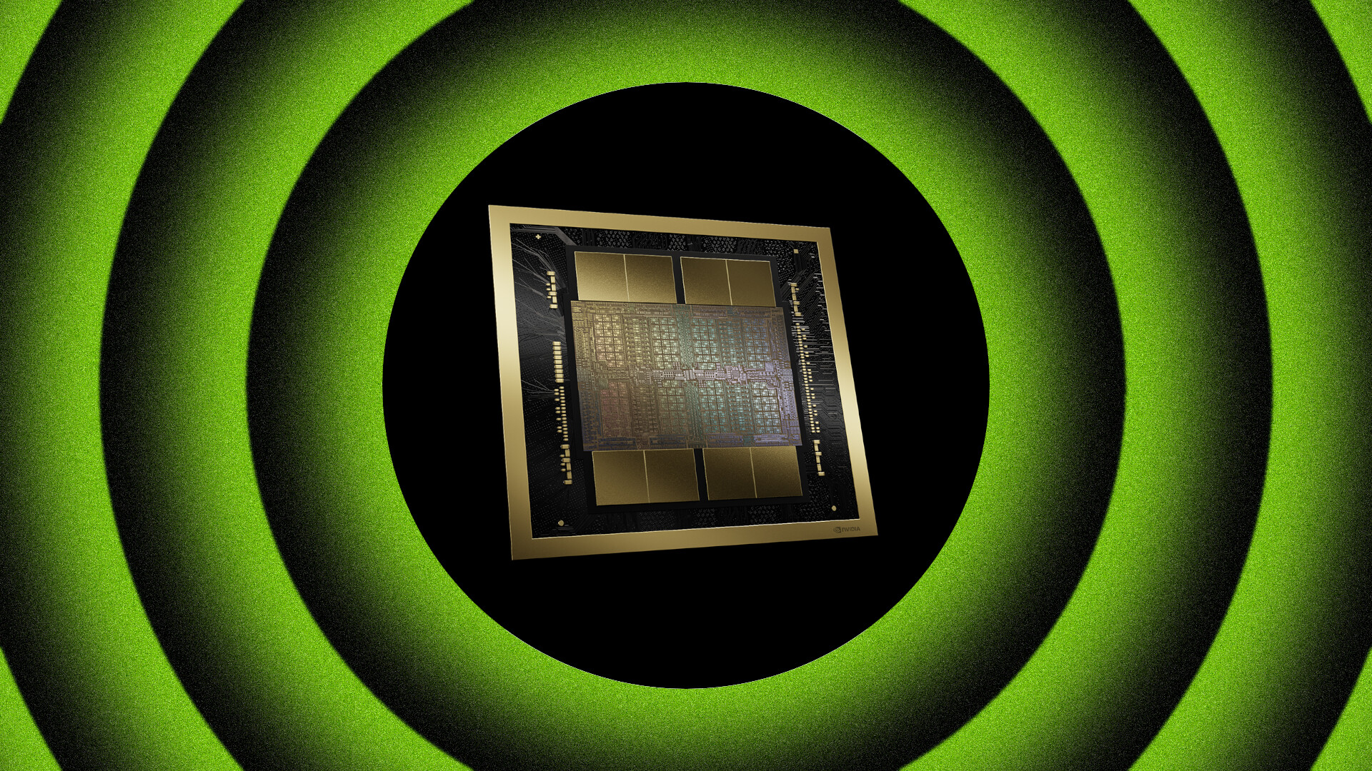
Following Monday's blockbuster announcements of the "Blackwell" architecture and NVIDIA's B100, B200, and GB200 AI GPUs, all eyes are now on its client graphics derivatives, or the GeForce RTX GPUs that implement "Blackwell" as a graphics architecture. Leading the effort will be the new GB202 ASIC, a successor to the AD102 powering the current RTX 4090. This will be NVIDIA's biggest GPU with raster graphics and ray tracing capabilities. The GB202 is rumored to be followed by the GB203 in the premium segment, the GB205 a notch lower, and the GB206 further down the stack. Kopite7kimi, a reliable source with NVIDIA leaks, says that the GB202 silicon will be built on the same TSMC 4N foundry node as the GB100.
TSMC 4N is a derivative of the company's mainline N4P node, the "N" in 4N stands for NVIDIA. This is a nodelet that TSMC designed with optimization for NVIDIA SoCs. TSMC still considers the 4N as a derivative of the 5 nm EUV node. There is very little public information on the power- and transistor density improvements of the TSMC 4N over TSMC N5. For reference, the N4P, which TSMC regards as a 5 nm derivative, offers a 6% transistor-density improvement, and a 22% power efficiency improvement. In related news, Kopite7kimi says that with "Blackwell," NVIDIA is focusing on enlarging the L1 caches of the streaming multiprocessors (SM), which suggests a design focus on increasing the performance at an SM-level.
Sources:
Kopite7kimi (Twitter), #2, VideoCardz
TSMC 4N is a derivative of the company's mainline N4P node, the "N" in 4N stands for NVIDIA. This is a nodelet that TSMC designed with optimization for NVIDIA SoCs. TSMC still considers the 4N as a derivative of the 5 nm EUV node. There is very little public information on the power- and transistor density improvements of the TSMC 4N over TSMC N5. For reference, the N4P, which TSMC regards as a 5 nm derivative, offers a 6% transistor-density improvement, and a 22% power efficiency improvement. In related news, Kopite7kimi says that with "Blackwell," NVIDIA is focusing on enlarging the L1 caches of the streaming multiprocessors (SM), which suggests a design focus on increasing the performance at an SM-level.
60 Comments on NVIDIA "Blackwell" GeForce RTX to Feature Same 5nm-based TSMC 4N Foundry Node as GB100 AI GPU
The biggest outlier in recent generations was Turing (20xx) in late 2018 on TSMC 12 nm (FinFET), which was just optimized node of 2016 Pascal (10xx), with also basically no raster uplift, the only real generational change was inclusion of tensor cores for RTX, DLSS, which took a long time for game designers to actually implement (and by that time 20xx was basically obsolete).
1. If that includes Increase to die size, it's not an aggerate since.
2. if that include an increase in clock speed, it not aggerate either.
I mean, by the same-ish metric Zen 4 is what, only a couple of percent faster than Zen 3? Since if we lock two single-CCD chips to same frequency and run CB or something that would be the result. However, nobody sane is saying that Zen 4 is a minor at best improvement over Zen 3, right?
If you want a great history lesson, and I highly recommend that you might, check out reviews on NV40 and NV45 in relation to NV38. There you will find your 40% clock-for-clock, millimeter-for-millimeter increase.
I pulled aggregate increases off launch-day reviews. Obviously in some of those performance metrics the 6800 did not do well, because driver maturity is a big factor. That's something Rankine never received because it was stuck on its lopsided implementation of DX9a and required per-game tuning to achieve proper scaling from the architecture. Curie is full DX9c and received plentiful driver and software improvements, allowing later performance to eclipse Rankine's by as much as 2.2x. This is why the improvement is aggregated; architectural changes exceed just more transistors more better. NVIDIA was still designing chips using EDL programming and that allowed fundamental changes for very little transistor cost every time the programming model was updated. Designs for SM3.0 were a paradigm shift in that regard.
Rankine's FP forward architecture and dual-issue (2fp/1int) scalar pipelines are an interesting rabbit hole to fall down if you want to see the pitfalls of ASIC design by programming limits. NVIDIA could only ever extract 8px/clock in one or two extremely niche scenarios while the TMU arrangement languished waiting for tex fetches.
This is more like the jump from Kepler to Maxwell.
I do think there's a fair amount of room to extract more performance from the same node, though, but not 100% like that one leaker on twitter claimed.
It did seem like with the density increase from Sam 8nm to 4N that Nvidia was not able to extract all the performance they could out of that node. As far as the die size goes, they can go bigger but not much more than 20% bigger. 20% bigger put the GB202 die into TU102 territory.
A cut down GB202, 20-25% faster than 4090 and they call it a day.
See you in 2027 again.