Wednesday, October 7th 2026

Samsung Foundry to Manufacture Anthropic AI ASIC on 2 nm Node
Samsung Foundry may be on the verge of securing a significant deal with AI lab Anthropic to manufacture AI accelerators. According to the latest report, Anthropic is developing its custom AI accelerator on Samsung's SF2 2 nm node, which will initially be produced in a lower volume of around 200,000 chips. The design and implementation of this ASIC are being handled by Broadcom, targeting around 4,000 TOPS of INT8 compute, with a TDP of 1,300 W per chip. This will be supported by either 192 GB of HBM3E or even 288 GB of HBM3E, if the design allows. The current production volume is low, as ASIC projects are typically counted in millions of chips. However, Anthropic is likely evaluating the project's viability, which requires a complete custom infrastructure with networking, rack design, power supply, cooling, and many other factors.
The current Samsung SF2 node is built using Low-NA EUV lithography and is manufactured in South Korea, with a new facility soon to be established in Taylor, Texas. For packaging these chips and integrating them with HBM, Samsung is likely to employ its I-Cube technology, which rivals TSMC's CoWoS and allows for 2.5D packaging. Combined with the 2 nm dies, Samsung can position itself as a serious manufacturing plant for external customers and slightly close the gap with TSMC and its contract manufacturing business.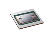 Additionally, Samsung and Qualcomm are reportedly forming a 2.1D Packaging Alliance to provide customers with access to advanced chip packaging using bridges that connect silicon dies. This new 2.1D packaging alliance will use organic bridges made from materials commonly found in traditional PCBs, such as organic polymer materials like epoxy and copper wiring, to interconnect multiple chips. Samsung might use this packaging technology as well, but more information will likely emerge as this chip gets closer to a tapeout.
Source:
via Jukan on X
The current Samsung SF2 node is built using Low-NA EUV lithography and is manufactured in South Korea, with a new facility soon to be established in Taylor, Texas. For packaging these chips and integrating them with HBM, Samsung is likely to employ its I-Cube technology, which rivals TSMC's CoWoS and allows for 2.5D packaging. Combined with the 2 nm dies, Samsung can position itself as a serious manufacturing plant for external customers and slightly close the gap with TSMC and its contract manufacturing business.

9 Comments on Samsung Foundry to Manufacture Anthropic AI ASIC on 2 nm Node
I can't, for the life of me, think it is normal when the tech magnates promise multi-GW clusters everywhere when both power generation and transmission capacity ain't there.
Broadcom are designing ai chips for openai as well, wonder where the funding is coming from this time?