Report an Error


NVIDIA GF110
GF110

GF110-040-A1

GF110-270-A1
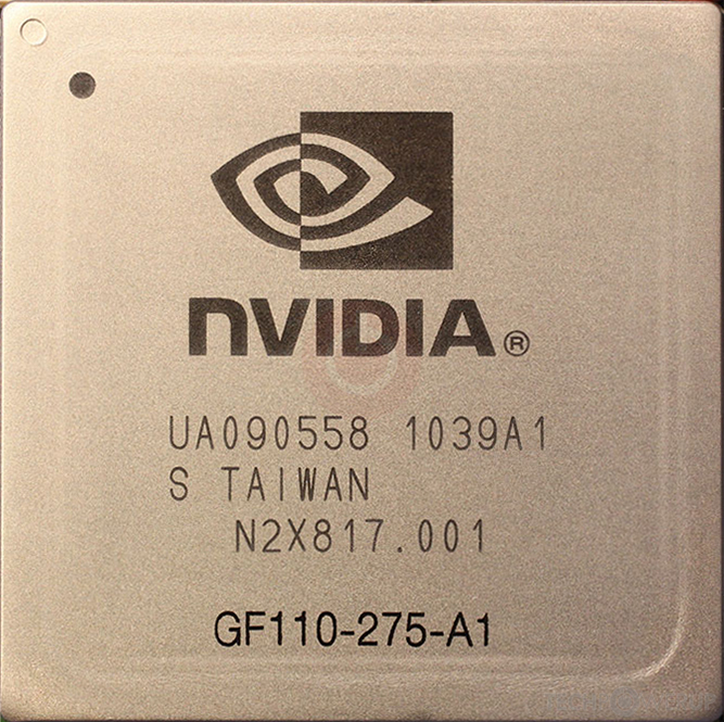
GF110-275-A1
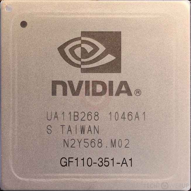
GF110-351-A1

GF110-375-A1

GF110-380-A1
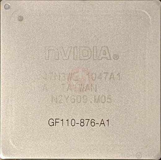
GF110-876-A1

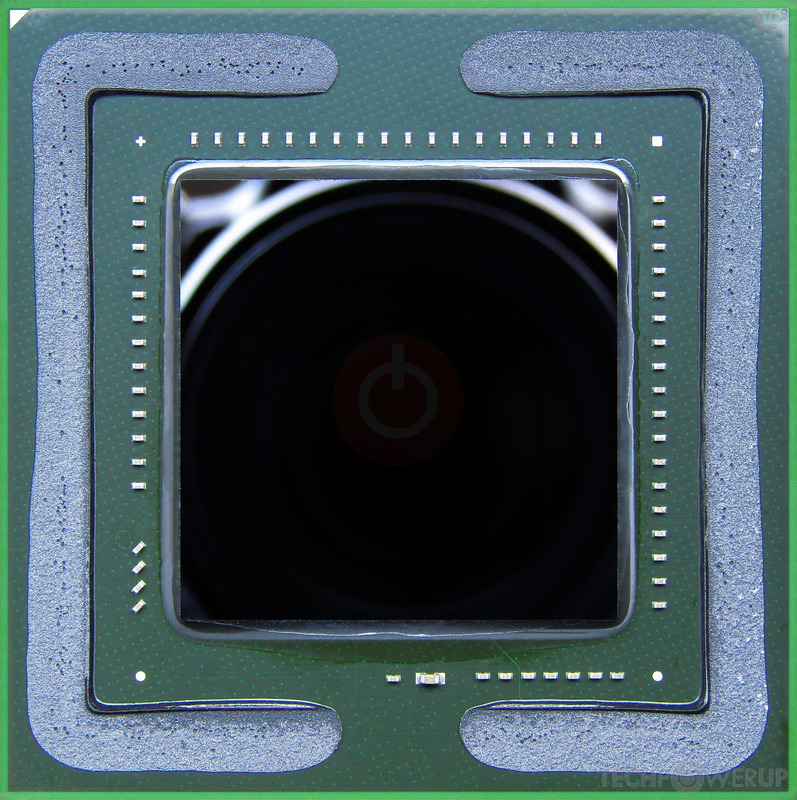
Fritzchens Fritz
Die Shot
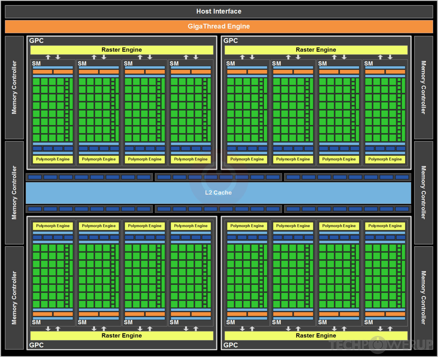
Block Diagram
SM Diagram
NVIDIA's GF110 GPU uses the Fermi 2.0 architecture and is made using a 40 nm production process at TSMC. With a die size of 520 mm² and a transistor count of 3,000 million it is a very big chip. GF110 supports DirectX 12 (Feature Level 11_0). For GPU compute applications, OpenCL version 1.1 and CUDA 2.0 can be used. It features 512 shading units, 64 texture mapping units and 48 ROPs.
Further reading:
Fermi Compute Architecture 
Graphics Processor
- Released
- Nov 9th, 2010
- GPU Name
- GF110
- Codename
- NVC8
- Architecture
- Fermi 2.0
- Foundry
- TSMC
- Process Size
- 40 nm
- Transistors
- 3,000 million
- Density
- 5.8M / mm²
- Die Size
- 520 mm²
- Package
- BGA-1981
Graphics Features
- DirectX
- 12 (11_0)
- OpenGL
- 4.6
- OpenCL
- 1.1
- Vulkan
- N/A
- CUDA
- 2.0
- Shader Model
- 5.1
- WDDM
- 2.3
- PureVideo HD
- VP4
- VDPAU
- Feature Set C
Render Config
- Shading Units
- 512
- TMUs
- 64
- ROPs
- 48
- SM Count
- 16
- SFUs
- 64
- GPCs
- 4
- L1 Cache
- 64 KB per SM
- L2 Cache
- 768 KB
- Max. TDP
- 600 W
All Fermi 2.0 GPUs
NVIDIA GPU Architecture History
- 2024 Blackwell
- 2023 Hopper
- 2022-2024 Ada Lovelace
- 2020-2024 Ampere
- 2018-2022 Turing
- 2017-2020 Volta
- 2016-2021 Pascal
- 2014-2019 Maxwell 2.0
- 2014-2017 Maxwell
- 2013-2015 Kepler 2.0
- 2012-2018 Kepler
- 2010-2016 Fermi 2.0
- 2010-2013 VLIW Vec4
- 2010-2016 Fermi
- 2007-2013 Tesla 2.0
- 2006-2010 Tesla
- 2003-2013 Curie
- 2003-2005 Rankine
- 2001-2003 Kelvin
- 1999-2005 Celsius
- 1998-2000 Fahrenheit
Graphics cards using the NVIDIA GF110 GPU
| Name | Chip | Memory | Shaders | TMUs | ROPs | GPU Clock | Memory Clock |
|---|---|---|---|---|---|---|---|
| GF110-275-A1 | 1280 MB | 480 | 60 | 40 | 732 MHz | 950 MHz | |
| GF110-375-A1 | 1536 MB | 512 | 64 | 48 | 772 MHz | 1002 MHz | |
| GF110-351-A1 | 1536 MB | 512 | 64 | 48 | 608 MHz | 854 MHz | |
| GF110-270-A1 | 1280 MB | 448 | 56 | 40 | 732 MHz | 950 MHz | |
| GF110-351-A1 | 6 GB | 448 | 56 | 48 | 574 MHz | 783 MHz | |
| 1280 MB | 352 | 44 | 40 | 732 MHz | 950 MHz | ||
| GF110-040-A1 | 1280 MB | 384 | 48 | 40 | 552 MHz | 802 MHz | |
| 6 GB | 512 | 64 | 48 | 574 MHz | 750 MHz | ||
| N12E-Q5-A1 | 4 GB | 384 | 48 | 32 | 450 MHz | 650 MHz | |
| 6 GB | 512 | 64 | 48 | 651 MHz | 924 MHz | ||
| 6 GB | 512 | 64 | 48 | 651 MHz | 851 MHz | ||
| 6 GB | 512 | 64 | 48 | 651 MHz | 924 MHz | ||
| GF110-876-A1 | 6 GB | 448 | 56 | 48 | 574 MHz | 783 MHz | |
| 6 GB | 512 | 64 | 48 | 651 MHz | 924 MHz | ||
| GF110-380-A1 | 1536 MB | 512 | 64 | 48 | 772 MHz | 1002 MHz | |
| GF110-275-A1 | 1280 MB | 480 | 60 | 40 | 732 MHz | 950 MHz |


GF110 GPU Notes
| PureVideo HD: VP4 VDPAU: Feature Set C GF110 has 4 GPCs each capable of 8 pixels per clock. This limits complete GPU to 32 pixels per clock and because of that it can't feed all 48 ROPs when they all require data at the same time. Additional ROPs however can be used for MSAA (because it doesn't require additional data from rasterizers, while giving more work to ROPs.) The complete die contains 64 texture address units and 256 texture filtering units. |
Apr 26th, 2024 09:04 EDT
change timezone
Latest GPU Drivers
New Forum Posts
- The Official Linux/Unix Desktop Screenshots Megathread (696)
- What are you playing? (20538)
- Horizontal black lines popping up on my screen? (12)
- Which new games will you be buying? (321)
- GoDeal24 Windows 11 Pro 32-bit! (3)
- Secure boot already open help (3)
- What's your latest tech purchase? (20349)
- Alphacool CORE 1 CPU block - bulging with danger of splitting? (24)
- Old high quality PSU, or semi-old mid-quality PSU? (1)
- Best SSD for system drive (86)
Popular Reviews
- HYTE THICC Q60 240 mm AIO Review
- MOONDROP x Crinacle DUSK In-Ear Monitors Review - The Last 5%
- Alienware Pro Wireless Gaming Keyboard Review
- Upcoming Hardware Launches 2023 (Updated Feb 2024)
- Thermalright Phantom Spirit 120 EVO Review
- ASUS Radeon RX 7900 GRE TUF OC Review
- FiiO K19 Desktop DAC/Headphone Amplifier Review
- RTX 4090 & 53 Games: Ryzen 7 5800X vs Ryzen 7 5800X3D Review
- NVIDIA RTX 4090: 450 W vs 600 W 12VHPWR - Is there any notable performance difference?
- RTX 4090 & 53 Games: Core i9-13900K vs Ryzen 7 5800X3D Review
Controversial News Posts
- Windows 11 Now Officially Adware as Microsoft Embeds Ads in the Start Menu (123)
- Sony PlayStation 5 Pro Specifications Confirmed, Console Arrives Before Holidays (117)
- NVIDIA Points Intel Raptor Lake CPU Users to Get Help from Intel Amid System Instability Issues (106)
- AMD "Strix Halo" Zen 5 Mobile Processor Pictured: Chiplet-based, Uses 256-bit LPDDR5X (101)
- US Government Wants Nuclear Plants to Offload AI Data Center Expansion (98)
- AMD's RDNA 4 GPUs Could Stick with 18 Gbps GDDR6 Memory (89)
- Developers of Outpost Infinity Siege Recommend Underclocking i9-13900K and i9-14900K for Stability on Machines with RTX 4090 (85)
- Windows 10 Security Updates to Cost $61 After 2025, $427 by 2028 (84)