Report an Error


AMD RV670
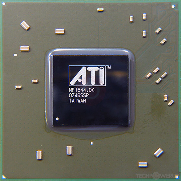
RV670

Die Shot

Block Diagram
AMD's RV670 GPU uses the TeraScale architecture and is made using a 55 nm production process at TSMC. With a die size of 192 mm² and a transistor count of 666 million it is a small chip. RV670 supports DirectX 10.1 (Feature Level 10_1). For GPU compute applications, OpenCL version N/A can be used. It features 320 shading units, 16 texture mapping units and 16 ROPs.
Further reading:
R600 Series Instruction Set Architecture 
Graphics Processor
- Released
- Nov 8th, 2007
- GPU Name
- RV670
- Mobile Variant
- M88
- Codename
- Boom
- Architecture
- TeraScale
- Foundry
- TSMC
- Process Size
- 55 nm
- Transistors
- 666 million
- Density
- 3.5M / mm²
- Die Size
- 192 mm²
- Package
- FCBGA-1281
Graphics Features
- DirectX
- 10.1 (10_1)
- OpenGL
-
3.3 (full)
4.0 (partial)
- OpenCL
- N/A
- Vulkan
- N/A
- Shader Model
- 4.1
- WDDM
- 1.1
- Compute
- GFX3
- DCE
- 2.0
- UVD
- 1.0
Render Config
- Shading Units
- 320
- TMUs
- 16
- ROPs
- 16
- Compute Units
- 4
- Z-Stencil
- 32
- Vertex Cache
- 32 KB
- Texture Cache
- 32 KB
- Tex L1 Cache
- 32 KB per 4 SPs
- L2 Cache
- 256 KB
- Max. TDP
- 105 W
All TeraScale GPUs
- ATI M72
- ATI M74
- ATI M76
- ATI M82
- ATI M84
- ATI M86
- ATI M88
- ATI M92
- AMD M93
- ATI M93
- ATI M96
- ATI M97
- ATI M98
- ATI R600
- ATI R680
- ATI R700
- ATI RS780
- ATI RS880
- ATI RV610
- ATI RV620
- ATI RV630
- ATI RV635
- ATI RV670
- AMD RV670
- ATI RV710
- AMD RV711
- ATI RV711
- ATI RV730
- ATI RV740
- ATI RV770
- AMD RV770
- ATI RV790
- ATI RX881
- ATI Theater 650 PRO
- ATI Xenos Corona
- ATI Xenos Falcon
- ATI Xenos Jasper
- ATI Xenos Vejle
- ATI Xenos Xenon
AMD GPU Architecture History
- 2023 CDNA 3.0
- 2022-2024 RDNA 3.0
- 2021 CDNA 2.0
- 2020 CDNA 1.0
- 2020-2023 RDNA 2.0
- 2019-2020 RDNA 1.0
- 2018-2022 GCN 5.1
- 2017-2020 GCN 5.0
- 2016-2020 GCN 4.0
- 2014-2019 GCN 3.0
- 2013-2017 GCN 2.0
- 2011-2020 GCN 1.0
- 2010-2013 TeraScale 3
- 2009-2015 TeraScale 2
- 2005-2013 TeraScale
- 2005-2007 Ultra-Threaded SE
Graphics cards using the AMD RV670 GPU
| Name | Chip | Memory | Shaders | TMUs | ROPs | GPU Clock | Memory Clock |
|---|---|---|---|---|---|---|---|
| 2 GB | 320 | 16 | 16 | 777 MHz | 802 MHz |

RV670 GPU Notes
| Mobile Variant: M88 Codename: Boom Graphics/Compute: GFX3 Display Core Engine: 2.0 Unified Video Decoder: 1.0 |
May 8th, 2024 04:55 EDT
change timezone
Latest GPU Drivers
New Forum Posts
- POLL: Can you see the difference past 60fps (gaming/other) (21)
- TPU's Nostalgic Hardware Club (18497)
- Your way of cooling your PC? (3)
- Does anyone here overclock their video cards? Is it really worth it? (31)
- High c0% and system idle process (1)
- Free Games Thread (3787)
- Nerdy year long streaming saga [ XD probably] (2)
- I wonder how much performance could be gained with m4 chip in iPad pro OLED, if it had an AirJet (1)
- PSU making a clicking sound, PC wont turn on (14)
- Technical Issues - TPU Main Site & Forum (2024) (54)
Popular Reviews
- CHERRY XTRFY M64 Pro Review
- Corsair iCUE Link RX120 RGB 120 mm Fan Review
- Finalmouse UltralightX Review
- Upcoming Hardware Launches 2023 (Updated Feb 2024)
- Cougar Hotrod Royal Gaming Chair Review
- Meze Audio LIRIC 2nd Generation Closed-Back Headphones Review
- AMD Ryzen 7 7800X3D Review - The Best Gaming CPU
- ASRock NUC BOX-155H (Intel Core Ultra 7 155H) Review
- ASUS Radeon RX 7900 GRE TUF OC Review
- Sapphire Radeon RX 7900 GRE Pulse Review
Controversial News Posts
- Intel Statement on Stability Issues: "Motherboard Makers to Blame" (259)
- AMD to Redesign Ray Tracing Hardware on RDNA 4 (203)
- Windows 11 Now Officially Adware as Microsoft Embeds Ads in the Start Menu (167)
- NVIDIA to Only Launch the Flagship GeForce RTX 5090 in 2024, Rest of the Series in 2025 (137)
- Sony PlayStation 5 Pro Specifications Confirmed, Console Arrives Before Holidays (119)
- AMD's RDNA 4 GPUs Could Stick with 18 Gbps GDDR6 Memory (114)
- NVIDIA Points Intel Raptor Lake CPU Users to Get Help from Intel Amid System Instability Issues (106)
- AMD Ryzen 9 7900X3D Now at a Mouth-watering $329 (104)