Monday, November 3rd 2025

More Evidence for AVX10 and APX Support in Intel "Nova Lake" Emerge

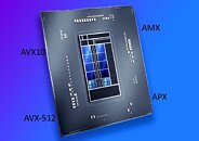
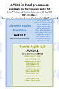
Intel's advanced features like AVX10, APX, and AMX instruction sets—designed for 512-bit acceleration and fast vector/matrix multiplication for tasks such as content creation, encoding/decoding, and AI—may not be exclusive to Intel Xeon processors. We could potentially see them in consumer "Nova Lake" processors. According to the Netwide Assembler (NASM), an assembler for the x86 CPU, Nova Lake might introduce these features in consumer PCs once again. A few weeks ago, it was believed that Nova Lake wouldn't include any of Intel's advanced x86 extensions. The latest GCC compiler patch indicated that the initial Nova Lake enablement does not incorporate AVX10, AMX, or APX. This suggested that support for these new x86 instructions might be absent from the next-generation CPU.

Initially, Intel chose to disable AVX-512 for the "Alder Lake" and "Raptor Lake" client-oriented CPU lineups, meaning that only server-grade Xeon CPUs benefited from the accelerated 512-bit data paths. With the release of NASM 3.0 and its subsequent 3.1 update, we are once again optimistic that Nova Lake will bring 512-bit acceleration to its client CPUs. Rumored to feature up to 52 cores, including 16 P-Cores, 32 E-Cores, and 4 LPE-Cores, Nova Lake could be an ideal CPU for gaming and workstation tasks, covering a wide range of scenarios and workloads, except for server applications, which are reserved for Xeon. Additionally, it could take advantage of the extensive ecosystem of AVX-accelerated software available today.
For reference, AMD introduced full AVX-512 support with its "Zen 5" cores across its product range, providing a performance boost in optimized applications for both desktop and server CPUs. This marked the first time AMD did not emulate 512-bit AVX, which previously required splitting 512-bit data into two 256-bit units to be processed over two cycles. If Intel reintroduces full AVX-512 acceleration in its client SoCs, it will mark the first time both companies offer 512-bit vector acceleration in their consumer CPUs simultaneously.
Source: @InstLatX64 on X
Add your own comment

36 Comments on More Evidence for AVX10 and APX Support in Intel "Nova Lake" Emerge

#27
Nhonho
stevegalaxiusavx-512 was first introduced with skylake-X with the X series of processors, in late 2016. They were rebadged xeons. skylake consumer chips and skylake server chips actually have a completely different core architecture with significant differences, the most notably being an entirely different mesh topography that has the cores arranged in a large grid so they can communicate with each other faster. this was to get around the latency issues that high core count broadwell server chips with higher core counts using a traditional ring topography. The core design in the server chips also has a completely different caching structure to feed the large data throughput of avx-512, which is why they have a large l2 cache and a small l3 cache and the l3 cache isn't inclusive.

Part of the reason the core design is different is also because the first implementation of avx-512 was an extension of their cpu-as-a-gpu project called Knights Landing (which is where the mesh topography came from) and extremely experimental. the massive dual execution units take up a large amount of the die area and required very beefy power delivery to keep the ridiculous number of transistors active, which meant that they downclocked heavily when avx-512 was active.

There is very little software that takes advantage of these instructions, and half of that software is also heavily dependent on the implementation because the first generation of chips was basically geared toward research use.
AVX-512 instructions were present in the cores of Skylake home CPUs (Core 6000 series), but were disabled at the factory. Back then, it took several years to start and finish a core design; nowadays, core design takes much less time to complete because it's accelerated by AI. And even today, the design of cores for home and server CPUs is the same; what changes is that the factory (Intel and AMD) disables some "server features" in CPUs that will be sold to the home market.
Dr. DroThis is a convenient support matrix for AVX-512 subsets, as mentioned earlier, Skylake doesn't support it.
Obviously that the Core 6000 series won't appear in this table because AVX-512 instructions were disabled on them at the factory.
Posted on Reply
#28
Rulumi
NhonhoAVX-512 instructions were present in the cores of Skylake home CPUs (Core 6000 series), but were disabled at the factory. Back then, it took several years to start and finish a core design; nowadays, core design takes much less time to complete because it's accelerated by AI. And even today, the design of cores for home and server CPUs is the same; what changes is that the factory (Intel and AMD) disables some "server features" in CPUs that will be sold to the home market.
Skylake-S and all of its derivates have some clearly visible unused and empty areas inside the core parts in the die that are related to AVX-512.


Sources of the photos:
chipsandcheese.com/p/skylake-intels-longest-serving-architecture
Posted on Reply
#29
igormp
If all cores support it (even if double pumped on the E-cores), with those core counts and a fast enough memory subsystem to keep it up, this should be a beast at productivity.
qcmadnessDoes that mean "emulating" ABX-512 in author's view?
which previously required splitting 512-bit data into two 256-bit units to be processed over two cycles.
Basically double pumping.
ToTTenTranzWhat's using AVX512 nowadays? Honest question. It's faster for some ML workloads, but those are completely offloaded to NPUs and GPUs nowadays.
Not everything is offloaded to NPUs/GPUs, lots of the pre-processing, specially for images, is often done on the CPU, and vector instructions helps a LOT in those scenarios.
Compression/decompression and crypto tasks also can make use of AVX-512 for some extra gains, and those take place in lots of places.
kondaminAVX512 requires a lot of power, so much so that the moment they hit the cpu has to throttle.
It used to be really bad in terms of throttling and power consumption, but newer implementations basically solved that, see:

www.numberworld.org/blogs/2024_8_7_zen5_avx512_teardown/#throttling

AVX-512 actually uses less power than regular AVX and SSE, mostly due to throttling, but still manages to finish the tasks way faster.
Here's a longer writeup on Zen 5's AVX-512 behaviour:
chipsandcheese.com/p/zen-5s-avx-512-frequency-behavior

Intel's current AVX-512 implementations have also pretty much solved the power and throttling issues.
Posted on Reply
#30
tony164
ToTTenTranzWhat's using AVX512 nowadays?
It's automatically used by Java JIT and C/C++/Rust compilers if enabled by compilation target, so you can benefit from it even without changing a single line of code. It's also being used in all kinds of string processing now, including JSON parsing (check out simdjson), etc.

It's a common misconception that AVX512 is only relevant for special workloads or for its wider 512-bit registers. But AVX512 introduced a lot more instructions that are beneficial for all sorts of (smaller) use cases and also work on (double the number of) 128 and 256-bit registers, and if you don't use 512-bit operations, there's no throttling and it's just as—if not more—efficient as AVX2. With modern implementations there's no longer a frequency penalty like there used to be with older Intel CPUs, so there's basically no downside in using AVX512.
By now, the main thing still holding it back is the lack of widespread hardware support and the need to support older hardware still.
Posted on Reply
#31
Nhonho
I'd like to know if the AVX10, AVX10.2, APX, and other instruction sets (and future sets as well) were developed solely by Intel or if they were developed in partnership with AMD.

I imagine that when certain technologies are developed jointly by both companies (AMD and Intel), the CPUs from both companies are released with the new technologies simultaneously, without either having priority over the technology's usage time.
Posted on Reply
#32
stevegalaxius
NhonhoAVX-512 instructions were present in the cores of Skylake home CPUs (Core 6000 series), but were disabled at the factory. Back then, it took several years to start and finish a core design; nowadays, core design takes much less time to complete because it's accelerated by AI. And even today, the design of cores for home and server CPUs is the same; what changes is that the factory (Intel and AMD) disables some "server features" in CPUs that will be sold to the home market.
there is space visible on the cores where part of the avx-512 register should be, but it is not physically present on the client skylake dies. It's just a blank spot. the server dies have a large portion of cache and the avx units added as a large block on top of the cores, and the register is not blank.
NhonhoI'd like to know if the AVX10, AVX10.2, APX, and other instruction sets (and future sets as well) were developed solely by Intel or if they were developed in partnership with AMD.

I imagine that when certain technologies are developed jointly by both companies (AMD and Intel), the CPUs from both companies are released with the new technologies simultaneously, without either having priority over the technology's usage time.
avx-512 was developed by intel around 2012 for the knights landing project which used special 54+ core cpus running systems on expansion cards like a GPU in large clusters. it was very strange.
Posted on Reply
#33
efikkan
Dr. DroThis is a convenient support matrix for AVX-512 subsets, as mentioned earlier, Skylake doesn't support it. Alder Lake does, but it is disabled in MCU and was fused off in newer manufacture CPUs, since they were not intended to support the feature (artificially). Raptor Lake and Arrow Lake CPUs have the extension set fused off from the factory.
It's only disabled in the front-end, the micro-ops on the back-end are still the same regardless of single operations, SSE or AVX. So there probably is a tiny benefit from the CPU optimizing 256-bit operations, which is also the case for CPUs fully supporting AVX-512, and is something to keep in mind when benchmarking software comparing AVX2 vs. AVX-512 - even the AVX2 code is benefiting a bit from it.

Some of you probably remember Alder Lake initially shipped with AVX-512 support enabled, and from what I can gather Intel originally intended for this to be handled in software. Unsurprisingly this didn't work flawlessly, leaving them the only option to disable it (although they could have left us the option…), and from what we've seen in recent AVX10.2 documentation they now plan to use the double-pumped approach for E-cores (also used by VIA and AMD). So why did Intel require so many generations fix this "defect"? Raptor Lake and Arrow Lake was already too far along in their development by the time they realized their mistake.
Dr. DroThat leaves Rocket Lake (11900K) and Ryzen 7000/9000 as the only client segment CPUs that can support it in some form.
As well as mobile Tiger Lake and Ice Lake, assuming we're not counting workstation chips.
Posted on Reply
#34
tony164
efikkan[...] and from what we've seen in recent AVX10.2 documentation they now plan to use the double-pumped approach for E-cores (also used by VIA and AMD). So why did Intel require so many generations fix this "defect"?
Not sure where you were going with this, but if you're asking why Intel didn't "just" use the double-pumped approach to support AVX512, well, they already did use it in their e-cores, except for 256-bit ops. So no, they can't do that until they have all 256-bit-wide execution units, and quad-pumping would not make sense. Also, not all instructions can be double-pumped.
Posted on Reply
#35
Draconis
NhonhoI'd like to know if the AVX10, AVX10.2, APX, and other instruction sets (and future sets as well) were developed solely by Intel or if they were developed in partnership with AMD.

I imagine that when certain technologies are developed jointly by both companies (AMD and Intel), the CPUs from both companies are released with the new technologies simultaneously, without either having priority over the technology's usage time.
It seems they are partnering. See here, and here
Posted on Reply
#36
tony164
NhonhoI'd like to know if the AVX10, AVX10.2, APX, and other instruction sets (and future sets as well) were developed solely by Intel or if they were developed in partnership with AMD.

I imagine that when certain technologies are developed jointly by both companies (AMD and Intel), the CPUs from both companies are released with the new technologies simultaneously, without either having priority over the technology's usage time.
I'm fairly sure AVX10 is solely from Intel. APX probably, too. I think there will be more collaboration or at least coordination for future extensions.
Posted on Reply
Add your own comment
Nov 15th, 2026 05:24 CST change timezone

New Forum Posts

Popular Reviews

TPU on YouTube

Controversial News Posts