Report an Error


ATI R580+
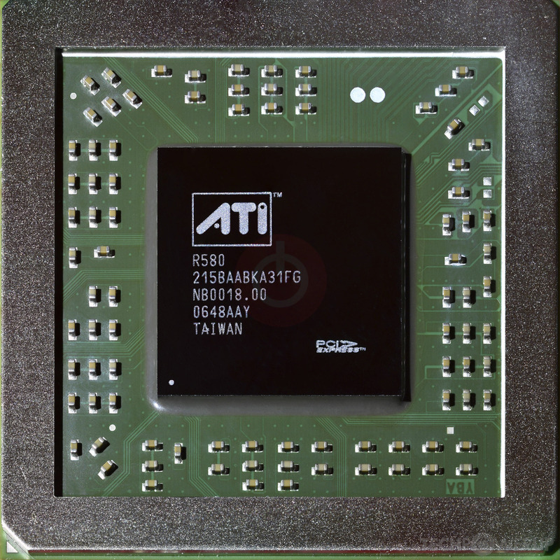
R580+

SIC66SIC66
Die Shot
ATI's R580+ GPU uses the Ultra-Threaded SE architecture and is made using a 90 nm production process at TSMC. With a die size of 352 mm² and a transistor count of 384 million it is a large chip. R580+ supports DirectX 9.0c (Feature Level 9_3). Modern GPU compute technologies are not available. It features 48 pixel shaders and 8 vertex shaders, 16 texture mapping units and 16 ROPs. Due to the lack of unified shaders you will not be able to run recent games at all (which require unified shader/DX10+ support).
Graphics Processor
- Released
- Sep 10th, 2006
- GPU Name
- R580+
- Codename
- Rodin
- Architecture
- Ultra-Threaded SE
- Foundry
- TSMC
- Process Size
- 90 nm
- Transistors
- 384 million
- Density
- 1.1M / mm²
- Die Size
- 352 mm²
Graphics Features
- DirectX
- 9.0c (9_3)
- OpenGL
-
2.1 (full)
3.0 (partial)
- OpenCL
- N/A
- Vulkan
- N/A
- Shader Model
- 3.0
- WDDM
- 1.0
- Compute
- GFX2
- DCE
- 1.0
Render Config
- Pixel Shaders
- 48
- Vertex Shaders
- 8
- TMUs
- 16
- ROPs
- 16
- Max. TDP
- 125 W
All Ultra-Threaded SE GPUs
ATI GPU Architecture History
Graphics cards using the ATI R580+ GPU
| Name | Chip | Memory | Shaders | TMUs | ROPs | GPU Clock | Memory Clock |
|---|---|---|---|---|---|---|---|
| R580+ XT | 512 MB | 48 / 8 | 16 | 16 | 650 MHz | 1000 MHz | |
| R580+ XT | 256 MB | 48 / 8 | 16 | 16 | 625 MHz | 900 MHz | |
| R580+ XT | 512 MB | 48 / 8 | 16 | 16 | 650 MHz | 1000 MHz | |
| R580+ XT | 256 MB | 48 / 8 | 16 | 16 | 625 MHz | 703 MHz | |
| R580+ XT | 512 MB | 48 / 8 | 16 | 16 | 670 MHz | 1050 MHz |


R580+ GPU Notes
| Codename: Rodin Graphics/Compute: GFX2 Display Core Engine: 1.0 Avivo Video Programmable pixel&vertex pipelines |
Apr 30th, 2024 15:14 EDT
change timezone
Latest GPU Drivers
New Forum Posts
- Would you guys be ok with 70C idle temp on NVME storage. (7)
- Is there a formula to help normalize temperature testing when ambient is variable? (14)
- Why MS buying all of these Studios is bad for Gaming (60)
- 7900 XTX Seriously lacking (69)
- HyperX mechanical keyboards (9)
- Using science and technology to cure tinnitus (ear ringing) (36)
- problem with my 7900xtx (13)
- i7-1355U (17)
- AMD RX 7000 series GPU Owners' Club (1091)
- RTX 4090? (25)
Popular Reviews
- Ugreen NASync DXP4800 Plus Review
- HYTE THICC Q60 240 mm AIO Review
- Team Group T-Force Vulcan ECO DDR5-6000 32 GB CL38 Review
- MOONDROP x Crinacle DUSK In-Ear Monitors Review - The Last 5%
- Upcoming Hardware Launches 2023 (Updated Feb 2024)
- Thermalright Phantom Spirit 120 EVO Review
- AMD Ryzen 7 7800X3D Review - The Best Gaming CPU
- FiiO K19 Desktop DAC/Headphone Amplifier Review
- ASUS Radeon RX 7900 GRE TUF OC Review
- Alienware Pro Wireless Gaming Keyboard Review
Controversial News Posts
- Intel Statement on Stability Issues: "Motherboard Makers to Blame" (188)
- Windows 11 Now Officially Adware as Microsoft Embeds Ads in the Start Menu (156)
- Sony PlayStation 5 Pro Specifications Confirmed, Console Arrives Before Holidays (117)
- AMD's RDNA 4 GPUs Could Stick with 18 Gbps GDDR6 Memory (108)
- NVIDIA Points Intel Raptor Lake CPU Users to Get Help from Intel Amid System Instability Issues (106)
- AMD "Strix Halo" Zen 5 Mobile Processor Pictured: Chiplet-based, Uses 256-bit LPDDR5X (103)
- US Government Wants Nuclear Plants to Offload AI Data Center Expansion (98)
- TechPowerUp Hiring: Reviewers Wanted for Motherboards, Laptops, Gaming Handhelds and Prebuilt Desktops (90)