News Posts matching #Intel

Return to Keyword Browsing

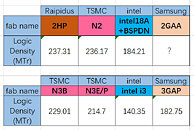
Rapidus 2HP 2 nm Node to Match TSMC N2 on Logic Density

According to Korean analyst Kurnal on X, Rapidus, the Japanese foundry pushing into leading-edge chips, will deliver its upcoming 2 nm process, called 2HP, with a transistor density that rivals the best in the business, even TSMC. The reporting allegedly shows a logic density of 237.31 million transistors per square millimeter for 2HP, essentially matching TSMC's N2, which has 236.17 MTr/mm², and comfortably ahead of Intel's 18A at about 184.21 MTr/mm². Rapidus has focused on high-density standard cells and a single-wafer front-end method that allows engineers to tune runs before scaling. It states that a 2 nm gate-all-around test chip built with ASML EUV tools met its electrical targets. The firm plans to publish process design kits in early 2026 and aims to start high-volume production at its IIM-1 facility in 2027, with monthly output expected to reach roughly 25,000 wafers.

What Rapidus is selling beyond raw density is speed and flexibility. While being a node or two behind TSMC in 2027, the company promises significantly shorter cycle times than traditional batch processes, reducing the typical turnaround from around 120 days to approximately 50 days, and offering extreme "hot lot" pushes down to 15 days for urgent orders. To deliver this, Rapidus is building a custom backend ecosystem with OSATs, EDA vendors, IP providers, and materials partners, and it benefits from government support and interest from major compute players. However, density is only one metric of the new node. Energy efficiency, performance per watt, mature supply chains, and, crucially, repeatable yields will determine whether Rapidus can turn validated test silicon into a reliable, high-volume competitor.
AAEON's UP Brand Announces Three New UP AI Dev Kits for AI Workloads

AAEON's UP brand, a leading provider of professional developer boards, today announced the release of a new line of AI development kit platforms based on its UP TWL, UP Squared Pro TWL, and UP Xtreme ARL, representing entry, mid, and high-end models. The new development kit series represents UP's first step on the roadmap outlined following the brand's 10-year anniversary, following which it reaffirmed its commitment to "Bridge the Gap from Idea to Success". This comes in light of the concurrent release of a full UP AI Ecosystem comprised of both hardware and software platforms designed to accelerate edge AI development from initial concept to mass production.

Representing the entry-level of the three, the UP TWL AI Dev Kit is positioned as a cost-effective, power-efficient option, which is also reflected in its Intel Processor N150 CPU (formerly Twin Lake). Sharing the same processor foundation, but with an integrated Hailo-8L, DEEPX DX-M1, or Axelera Metis AI acceleration module is the UP Squared Pro TWL AI Dev Kit. Courtesy of its versatile AI acceleration module support, the UP Squared Pro TWL AI Dev Kit offers up to 214 TOPS of AI inferencing performance with market-leading power-efficiency, reflecting its positioning as a kit for those wishing to bring AI functionality to low-power industrial projects.

Intel Patents Software-Defined Super Cores to Maximize Single-Core Performance

To maximize its CPU performance, Intel has filed a patent that describes a new way to boost single-thread performance by letting several smaller cores work together as if they were one larger core. Instead of chasing higher clock speeds or building ever-bigger cores, the idea is to dynamically fuse two or more physical cores so they cooperatively execute a single thread, while appearing to the operating system as a single logical core. The patent refers to this approach as Software Defined Super Cores, or SDC. The technique would split an instruction stream into chunks and hand those chunks to the fused cooperating cores. Those cores would coordinate closely, utilizing special buffers and fast communication paths to ensure correct memory ordering and data transfers. In heavier single-threaded cases, the processor can enter a fused mode, forming a "super core" that aggregates instructions per cycle without requiring higher voltage or frequency, which can improve performance per watt.

Keeping instructions in strict program order across multiple physical cores requires very low-latency inter-core messaging and careful synchronization, as well as scheduling the fused cores so they actually benefit real applications, which is a challenging software problem. Presumably, compiler magic would be needed to extract maximum bandwidth from this approach, which is something that made Intel's Itanium fail. If the approach can be made practical, it would give chip designers another way to scale single-thread performance beyond process shrinks and larger core designs. Whether we ever see an SDC design in shipping silicon will depend on the results of prototypes and how well operating systems and compilers can leverage the mode. Intel is constantly experimenting with new core architectures, but not everything makes it to volume production due to low feasibility.

Intel CFO Bets on "Nova Lake" to Close "Arrow Lake" Desktop Gap

At a Deutsche Bank technology conference, Intel CFO David Zinsner told investors that the company is placing its hopes on "Nova Lake" to repair weaknesses left by the current "Arrow Lake" lineup. He acknowledged the desktop family did not deliver the dollar-for-dollar competitiveness Intel wanted, even when unit shipments looked relatively strong. The Core Ultra 200 generation fell short in several high-profile gaming comparisons and experienced early stability issues that necessitated multiple firmware and software updates. Intel attempted to mitigate criticism with an approved overclocking program that allowed partners to ship validated boost profiles, but this effort did not fully address questions about the value of its flagship products. Zinsner called Nova Lake a broader, more complete set of SKUs that should help Intel recover market footing once the chips arrive in 2026.

Intel is pitching Nova Lake as more than a simple refresh, with redesigned cores, higher counts on select parts, and beefed-up integrated graphics aimed at the premium desktop segment. Independent testing and some early engineering samples will be needed to confirm real-world gains, so claims about performance remain unproven. Some enthusiasts may worry about another platform change, as Nova Lake will require a new socket, which complicates upgrade choices compared to platforms that promise longer longevity. Zinsner also noted parallel server roadmap adjustments, including a return to multi-threading and refinements to future Xeon families. For desktop buyers, the next year promises to be eventful as Intel tries to close the gap while rival AMD continues its own roadmap, shifting to Zen 6.

Intel Loses Advanced Packaging Director in Latest Executive Departure

Intel faces significant leadership challenges as a wave of veteran executives depart the company. Among the notable departures is Narahari Ramanuja, who dedicated 25 years to Intel, including over three years as Director of Advanced Packaging Technology Development, according to his LinkedIn profile. As reported by Oregon Live, Ramanuja will join Analog Devices as Managing Director and General Manager of their Beaverton FAB facility starting in late September. He joins Gang Duan, another Intel packaging expert who left for Samsung's components division, as reported by The Wall Street Journal, where Duan was recognized for his innovative contributions to semiconductor packaging technologies, particularly his work with glass materials.

The executive exodus occurs against a backdrop of massive workforce reductions and operational challenges for the chipmaker. According to Oregon Live, Intel has eliminated approximately 15,000 jobs in 2024, and 15,000 last month with Oregon bearing the brunt of these cuts—losing more than 5,400 positions over the past year alone. The departures extend beyond packaging specialists to include key manufacturing leadership, with Ann Kelleher, head of manufacturing, retiring in March, followed by Sanjay Natarajan, VP of factory technology research, in June, as noted by Oregon Live. Reuters reports that additional senior manufacturing executives, including corporate VPs Kaizad Mistry, Ryan Russell, and Gary Patton, are also set to retire. These changes come as Intel, despite recently agreeing to transfer a 10% stake to the U.S. government, continues pushing customers to adopt its Foveros advanced packaging technology over TSMC's CoWoS platform.

Former Asahi Linux GPU Driver Lead Jumps Ship to Intel GPU Driver Development

We've reported a handful of times about the Asahi Linux project, which aimed to bring Linux support to Apple Silicon MacBooks and desktops. A huge part of that mammoth task involved reverse engineering low-level items, like graphics drivers. Alyssa Rosenzweig was previously in charge of developing the open-source Mesa OpenGL/Vulkan drivers for the Asahi Linux project, but she recently announced her departure from the project and teased her involvement with the Intel HPG team.

Now, Rosenzweig has updated her resume with an entry titled "Designing open source graphics drivers for Intel GPUs." Rosenzweig's role at Intel will involve developing both Vulkan and OpenGL drivers for Intel GPUs on Linux, and there appears to be a specific focus on gaming. This could be an indication that Intel is planning to ramp up the development and performance of its graphics drivers on Linux, which has been slightly inconsistent on Intel's Arc dGPUs. The B580, for example, easily holds its own against GPUs like the AMD Radeon RX 7600 XT and NVIDIA GeForce RTX 4060 on Windows in our review, but on Linux, the B580 falls behind its peers by a significant margin in many instances. There have also been significant improvements in many games since the B580 launched, but it seems as though Intel is working on taking that even further with driver improvements.

Intel Releases Arc GPU Graphics Drivers 101.7028 Beta

Intel today released the latest version of Arc GPU Graphics Drivers. Version 101.7028 Beta comes with day-one "Game On" optimization for "Hell is Us" and "Metal Gear Solid Delta: Snake Eater." which release later this week. The drivers don't include any fixes with this release, given that it's a Beta that closely follows the 101.7026 WHQL release from earlier this week, but the company took the opportunity to identify new issues that will be fixed in future releases, such as issues released to "PEAK," "Broken Arrow," "World of Warcraft: Dragonflight," and PugetBench productivity benchmark. Grab the driver from the link below.

DOWNLOAD: Intel Arc GPU Graphics Drivers 101.7028 Beta

Intel Details "Clearwater Forest" Xeon with 288 E-Cores on 18A Process

Intel used Hot Chips to pull back the curtain on "Clearwater Forest", its next-generation E-core Xeon. The company has paired major architectural upgrades with its newest 18A process and advanced 3D Foveros packaging paired with EMIB. The chip replaces "Sierra Forest" and is built around the new "Darkmont" efficiency cores. Intel says Clearwater Forest will ship in a massive chiplet package using the 18A node for the compute pieces while relying on Foveros Direct 3D for stacking. The company is pitching this design as a showcase of what its foundry and packaging teams can now deliver.

Under the hood, the Darkmont E-core leans heavily on a wider, more parallel front end and a beefed-up out-of-order engine. Intel disclosed a 64 KB instruction cache per core and an expanded decoder that can handle more instructions per cycle than the previous "Crestmont" E-core design. Reorder and allocation structures have evolved, allocation units have been increased, and the out-of-order window has been enlarged to accommodate more in-flight work. Execution resources were also multiplied, with many more execution ports for integer and vector math, allowing the cores to sustain much higher parallel throughput.

Industrial ITX Motherboard from DFI Surfaces with Intel's Upcoming Panther Lake Processor

DFI has listed on its website a new ITX motherboard, the PTH171/PTH173, featuring Intel's upcoming Panther Lake-H processors. However, we should not be too excited, as the motherboard uses a 25 W TDP soldered CPU clearly oriented toward embedded systems rather than desktop usage. The lack of x16 PCIe slots indicates that all graphics processing relies on Panther Lake-H's integrated graphics capabilities. The motherboard offers one HDMI 2.0 port, one DisplayPort connection, one USB Type-C output, and one M.2-A display extension port supporting eDP, LVDS, HDMI, DVI, VGA, and DisplayPort interfaces. DFI PTH171/PTH173 motherboard feature two SODIMM slots that support DDR5-6400 and DDR5-7200 speeds, with a maximum of 128 GB. For storage and expansion, there is one PCIe Gen 5 x4 slot and several M.2 interfaces: an M Key for NVMe storage, a B Key for 4G/5G modules with a SIM slot, an E Key for Wi-Fi/Bluetooth, and an A Key for expanding display and USB options. Two additional M.2 slots are reserved for networking modules.

The I/O options are extensive: three Intel 2.5GbE connections, two COM ports, four USB 3.2 Gen 2 Type-A ports, one USB Type-C with DisplayPort Alternate Mode and 15 W power delivery, five USB 2.0 headers, two SATA 3.0 connections, and stereo audio with 3 W speaker output. For industrial use, the board includes full EXT-OOB support via DFI's own carrier board system to expand functionality, including optional internal RJ45 connectivity, CNVi integration, and compatibility with Intel vPro. DFI provides a 10-year lifecycle guarantee until Q1 2036, in line with Intel's roadmap. So far, we know that Intel's Panther Lake-H (PTL-H) is a mobile-focused chip that will debut on the Intel 18A process, alongside the main Panther Lake lineup and later Nova Lake CPUs. DFI's listing of a motherboard with a soldered PTL-H processor suggests that Intel has already begun shipping Panther Lake batches to partners, reinforcing the company's roadmap of a launch in the second half of 2025 followed by mass availability in 2026.

Intel Collaborates with LG Innotek to Implement an AI-powered Smart Factory

In the world of precision component manufacturing - think of the tiny parts inside modern cellphones, automotive car displays and other smart devices - being able to replicate the same part hundreds of thousands of times with perfect accuracy and zero defects has been a moonshot goal. Like many electronic component makers, LG Innotek, a South Korea-based global leader in materials and component manufacturing, aims to reach that goal with the help of innovative technology.

In LG Innotek's factory in Gumi, Korea, it will do that with an orchestra of Intel technologies: Intel Core processors, Intel Xeon processors and Intel Arc built-in graphics processing units (GPUs). It's all brought together with the OpenVINO software tool kit. While LG Innotek has long used both rule-based inspection and deep learning-based systems at specific terminals on its production lines to ensure higher product quality, LG aims to build a fully automated system without any performance degradations through the broad use of AI across every stage of the manufacturing process.

Intel Releases Arc GPU Graphics Drivers 101.7026 WHQL

Intel released the latest version of Arc GPU Graphics Drivers. Version 101.7026 WHQL comes with a handful of fixes. For the Arc B-series "Battlemage" discrete GPUs, it fixes a bug related to "Call of Duty: Black Ops 6" where the game exhibits corruption in some scenes with water graphics. Another bug fixed concerns "Final Fantasy XVI," where the game exhibits display corruption in some gameplay scenarios. The company also fixed the "Call of Duty: Black Ops 6" water artifacts bug for Intel Core Ultra Series 2 processors with Arc GPUs, namely "Lunar Lake," and "Arrow Lake-H." Grab the drivers from the link below.

DOWNLOAD: Intel Arc GPU Graphics Drivers 101.7026 WHQL

Intel and Trump Administration Reach Historic Agreement to Accelerate American Technology and Manufacturing Leadership

Intel Corporation today announced an agreement with the Trump Administration to support the continued expansion of American technology and manufacturing leadership. Under terms of the agreement, the United States government will make an $8.9 billion investment in Intel common stock, reflecting the confidence the Administration has in Intel to advance key national priorities and the critically important role the company plays in expanding the domestic semiconductor industry.

The government's equity stake will be funded by the remaining $5.7 billion in grants previously awarded, but not yet paid, to Intel under the U.S. CHIPS and Science Act and $3.2 billion awarded to the company as part of the Secure Enclave program. Intel will continue to deliver on its Secure Enclave obligations and reaffirmed its commitment to delivering trusted and secure semiconductors to the U.S. Department of Defense. The $8.9 billion investment is in addition to the $2.2 billion in CHIPS grants Intel has received to date, making for a total investment of $11.1 billion.

Intel Won't Abandon Glass Substrates, will License Tech to Externals

According to a report by South Korean outlet ETNews, cited by TrendForce, Intel has begun licensing its semiconductor glass substrate technology to external companies, marking a notable change in its business approach. As we reported this July, Intel had already signaled a retreat from producing glass substrates in-house, preferring instead to source finished solutions from specialized vendors. Intel is now reportedly in discussions with glass substrate makers, materials suppliers, and equipment providers about granting usage rights under defined terms in exchange for royalties. Rather than abandoning glass substrates, Intel appears to be repositioning itself as a technology licensor, allowing others to handle manufacturing while it benefits from its patent portfolio. This strategy, according to industry insiders, could accelerate wider market adoption by helping newcomers advance more quickly. Intel's shift is also seen as a response to ongoing issues in its manufacturing operations. By issuing licenses, the company can monetize its innovations while large-scale production is not expected until after 2030.

The glass substrate market is gaining momentum, with Absolics (an SKC subsidiary) already starting prototype production at its Georgia plant, which has an annual capacity of 12,000 square meters. Absolics plans to complete mass production setup by the end of 2025 and becoming the first to commercialize the technology. Meanwhile Samsung is preparing to adopt glass substrate interposers for advanced chips by 2028 and has established a pilot line at its Sejong facility. Major players such as Samsung Electronics, AMD, Broadcom, and Amazon are looking to adopt this technology, so Intel's decision may reshape the competitive landscape while creating new opportunities for collaboration.

Intel AI Playground Update Brings Prompt Edits, Advanced Video Generation, and More

Intel AI Playground version 2.6.0 has arrived with numerous practical updates that make experimenting with local generative models easier and more predictive. The release introduces new models, including GPT-OSS 20B, Wan 2.1 VACE, and Flux.1 Kontext into the Playground, and it updates core frameworks including OpenVINO, ComfyUI, and Llama.cpp. A new backend version control setting lets users choose which framework releases to install and run, so you can stay current between Playground updates. The standout workflow is Edit By Prompt, powered by Flux Kontext, which lets you change or combine images using plain language without manual masking. That means you can remove a microphone, turn a photo into anime, or merge two shots into a single cyberpunk scene just by describing the edit you want.

The update also expands video capabilities for systems with Intel Arc discrete GPUs, adding Image-to-Video and Video-to-Video workflows using Wan 2.1 VACE. The notes suggest starting at 512x512 pixels and about 49 frames to manage VRAM and iteration time, and they warn that a four-step LoRA setting can reduce compute at the cost of motion freedom. Convenience improvements include drag-and-drop thumbnails, a direct ComfyUI launch for node-level tweaks, Create and Enhance powered by PyTorch 2.8, Quick Access modes for Standard and HD, and a cleaner workflow menu. Image folders now use YYYYmmdd naming for easier sorting. Llama.cpp exposes an adjustable context size and a Vulkan backend for improved performance. Users can try more AI capabilities locally, and run their entire workflows from the central software.

Intel and AWS 8th Gen Amazon EC2 Instances Using Xeon 6 Are Now Available

Intel Xeon 6 processors with P-cores are now powering the new Amazon Elastic Compute Cloud (EC2) R8i and R8I-flex instances, available on AWS, delivering the highest performance and fastest memory bandwidth among comparable Intel processors in the cloud. The new instances reflect years of collaboration between Intel and AWS, bringing advanced silicon innovations and tightly integrated software optimizations to customers seeking scalable, cost-efficient and high-performance cloud infrastructure.

"The launch of the 8th Generation EC2 instances powered by Intel Xeon 6 is a milestone in our collaboration with AWS," said Ronak Singhal, senior fellow at Intel. "Together, we've built an infrastructure that accelerates AI, enhances memory performance, and simplifies deployment - helping customers achieve faster insights and stronger ROI."

Softbank Wanted to Buy Intel's Entire Foundry Division Before Settling for $2B Stake

Softbank wanted to buy out the entire foundry division of Intel, which the company refers to as Intel Foundry Services (IFS), but settled for a $2 billion equity stake in the company, Tom's Hardware reports citing Financial Times. This aligns with a long-held industry view that Intel is spinning off IFS as a standalone company much like AMD did with GlobalFoundries, about 15 years ago. Apparently, Softbank was stonewalled by Intel's CHIPS Act funding. In 2024, Intel entered an agreement with the US Department of Commerce to receive funding under the Biden Administration's CHIPS and Science Act. The company was granted $7.86 billion in funds on condition that Intel will maintain at least 50.1% stake in IFS if it ever sought to spin it off as a separate company.

China Modifies Intel Xeon 6P "Granite Rapids" Processors for Domestic Security

Montage Technology has unveiled the Jintide C6P CPU family, a line of server processors that repurpose Intel's "Granite Rapids" Xeon 6 design with added security and tracking features for the Chinese market. The company stated that the chips are designed for regulated sectors, including government, healthcare, and finance, where hardware-level controls and customizability are most critical. Montage framed the launch as the next step in a long-running collaboration that includes Tsinghua University and a special agreement with Intel, under which Montage can reconfigure and commercialize certain Xeon processors domestically. The C6P family maps to Intel's sixth-generation Xeon Scalable P-core lineup and appears to use Granite Rapids-SP silicon, the same foundation for Intel's Xeon 6700 and 6500 series.

Montage previously released a C6E series based on Sierra Forest E-cores and has now shifted to P-core parts for workloads that prioritize single-thread performance. Promotional images showed a C6787P, which follows Montage's convention of prefixing Intel SKUs with a C. The underlying Xeon 6787P is an 86-core, 172-thread design with roughly 336 MB of L3 cache. Platform features carried over from Granite Rapids include two-socket scalability, eight memory channels with support for high-speed DIMMs, many PCIe 5.0 lanes, and CXL 2.0 compatibility. Montage also states that it has embedded China-specific encryption, decryption, and monitoring capabilities at the chip level to meet local compliance requirements. This likely comes in the form of a nearby chip placed on the CPU package, below the ISH. The company has not yet published detailed specifications, pricing, or certification dates and has not confirmed whether the higher-core Granite Rapids-AP dies will be adapted to the domestic needs.

Intel to Bundle Battlefield 6 with Core Processors and Arc Graphics Cards

Intel announced that it is bundling "Battlefield 6" with select Core and Core Ultra processors, prebuilts powered by qualifying processor models, as well as select Arc graphics cards, mobile GPUs, and prebuilts that include them. The bundle is part of the 2025 Intel Gamer Days promotion under the company's Software Advantage Program. Select processor and graphics models will also include productivity software such as Canvid, Vegas Pro 365 (limited period subscription), and XSplit Premium Suite (limited period subscription). The game has an average retail value (ARV) of $69.99, while the software carry ARVs of $45, $19.99, and $60, respectively; for a total ARV of up to $194. As with most hardware bundles, the promotion is limited to select regions and participating retailers. The promotion purchase period is set from August 25 till September 14, 2025. An exhaustive list of processor and GPU models are covered in the promotion, listed below.

SoftBank Group and Intel Corporation Sign $2B Investment Agreement

SoftBank Group Corp.and Intel Corporation today announced their signing of a definitive securities purchase agreement, under which SoftBank will make a $2 billion investment in Intel common stock. The investment comes as both Intel and SoftBank deepen their commitment to investing in advanced technology and semiconductor innovation in the United States.

"Semiconductors are the foundation of every industry. For more than 50 years, Intel has been a trusted leader in innovation. This strategic investment reflects our belief that advanced semiconductor manufacturing and supply will further expand in the United States, with Intel playing a critical role," said Masayoshi Son, Chairman & CEO of SoftBank Group Corp. "We are very pleased to deepen our relationship with SoftBank, a company that's at the forefront of so many areas of emerging technology and innovation and shares our commitment to advancing U.S. technology and manufacturing leadership. Masa and I have worked closely together for decades, and I appreciate the confidence he has placed in Intel with this investment," said Lip-Bu Tan, CEO of Intel.

U.S. Government to Take a 10% Equity Stake in Intel

According to the latest report from Bloomberg, the U.S. government is currently discussing taking a 10% stake in Intel Corp. Late last week, we reported on Intel's CEO Lip-Bu Tan's visit to the White House to discuss the future of Intel as America's most important semiconductor manufacturer. And today, parts of the deal seem to be near completion, according to sources close to Bloomberg. Reportedly, some or all of Intel's CHIPS Act grants are going to be converted by the federal government into an equity stake in the company, which could help fuel further Intel Foundry expansion and R&D investments. Intel's CHIPS Act funding has reportedly not yet been reflected in the balance sheet, as the company has issued warnings in the past that these grants have been slow to arrive. However, under the new initiative, the U.S. government now plans to use this grant funding as a way to get equity in Intel Corp and become its largest shareholder with a 10% share.

Historically, Intel has been awarded roughly $10.9 billion in CHIPS Act grants for commercial and military applications. However, that funding hasn't materialized yet. What the U.S. now plans is a 10% stake, roughly worth $10.5 billion, which would practically mean the same thing, with voting power over company decisions as its largest stakeholder.

Intel "Bartlett Lake-S" Steppings Suggest Third Rebrand of "Raptor Lake" as "Bartlett Lake Hybrid"

"Bartlett Lake-S" is an interesting chip by Intel, given that its "Nova Lake-S" desktop processors with large L3 caches won't arrive before mid/late 2026. The chip is built on the idea that the "Raptor Cove" P-core offers gaming performance comparable or better to the "Lion Cove" P-cores implemented on "Arrow Lake-S." Intel figured that for a monolithic silicon with a similar die-size of "Raptor Lake-S," which has 8 P-cores and 4 E-core clusters, it could design a silicon with 12 P-cores for the same number of ring-stops, sharing the same 36 MB of L3 cache. A recent post on Twitter by Jaykihn highlights the stepping of this silicon as A0, but there's more to the story—apparently Intel will recycle its older "Raptor Lake" and "Alder Lake" silicon within "Bartlett Lake" generation, and refer to them as "Bartlett Lake Hybrid."

This "Bartlett Lake Hybrid" line of processors will reuse B0, C0, and H0 chips. The B0 chip is the original "Raptor Lake-S," which comes with an 8P+16E core-configuration, 36 MB of L3 cache, 2 MB of L2 cache per P-core, and 4 MB of L2 cache per E-core cluster. The C0 silicon is derived from "Alder Lake-S," with an 8P+8E config that has 1.25 MB of L2 cache per P-core and 2 MB of L2 cache per E-core cluster, with 30 MB of L3 cache. The H0 silicon originally drove the lower half of the 12th Gen Core family, it has 6 P-cores, each with 1.25 MB of L2 cache, no E-core clusters, and 18 MB of L3 cache.

New Intel "Lunar Lake" Core Ultra 7 254V SKU Appears

Intel's unannounced Core Ultra 7 254V has begun appearing in benchmark databases, and the figures suggest this may be a deliberately trimmed member of the "Lunar Lake" family, aimed at more affordable laptops. PassMark lists a multicore score of 17,327 and a single-core score of 4,089, which places the 254V noticeably behind the 256V and 258V in multithreaded work, while maintaining single-thread performance in line with other Core Ultra 7 chips. The listing also shows 12 MB of L3 cache and confirms an eight-core layout, matching Lunar Lake's standard design. Separate Furmark traces point to integrated Arc 140V graphics running at approximately 2.0 GHz, a GPU clock similar to that of higher-tier 7-series SKUs, which suggests that Intel may be binning an existing 256V to create a lower-cost option rather than designing something entirely new.

What remains unclear is the memory configuration, as Lunar Lake utilizes LPDDR5X packaged inside the SoC, and suffixes have so far indicated RAM capacity, with 2x8V mapping to 32 GB and 2x6V mapping to 16 GB. A 2x4V suffix would imply an even smaller memory option, but no confirmed devices are shipping with the 254V yet, and we don't know if a version with less than 16 GB memory has ever been planned/shipped. If Intel does release it, the chip could widen Lunar Lake's reach by offering efficient battery life and acceptable day-to-day performance at a lower price, making it an attractive choice for potential budget-focused buyers.

Intel Showcases Reference Arm-based SoC Manufactured on 18A Node

Intel Foundry has been releasing content on its products and services, and today, an interesting update came across. Intel showed a reference "Deer Creek Falls" SoC of what they call a "non-x86" design, manufactured on the 18A node. However, the design is actually Arm-based SoC. Consisting of seven cores, the reference SoC packs a single performance core, two efficiency cores, and four low-power efficiency cores, alongside the embedded PCIe and memory controller IPs and PHYs from ecosystem partners. While this may not be an impressive design, it demonstrates that a heterogeneous design of hybrid cores and IPs from ecosystem partners exists, and it's likely that we will see some designs emerging from this.

While Intel didn't explicitly mention that this SoC is Arm, later in the video, in the section on performance tuning, there are mentions of AArch64, which is Arm's designation for the 64-bit Arm ISA flavor. Alongside the design, Intel also demonstrated that the company offers a suite of performance optimization tools, even for Arm-based processors, allowing its customers to optimize and enhance software performance on their preferred platform, not just the x86 ISA. Hopefully, external foundry customers are slowly becoming aware of Intel Foundry's capabilities, and the scale can commence, especially now that Intel is under supervision from the U.S. government.

14:10 UTC: Update: Intel has delisted the video from its YouTube channel, but our screenshots remain.

Intel Enables Shared GPU Memory Override for iGPUs, Enables Larger Capacity

Intel has introduced a new driver feature called Shared GPU Memory Override, which allows integrated Arc GPUs on select Core Ultra systems to reserve a significantly larger portion of system RAM for video memory. The control appears in Intel Graphics Software as a slider that increases the percentage of system memory available to the iGPU. Early release notes and driver listings indicate default values near 57%, while vendor examples suggest that the control can allow significantly higher allocations on high-memory laptops, at 87% on Intel's demo. Intel positions the capability as a way to close the gap between integrated and discrete solutions for memory-bound graphics workloads and to give developers and power users greater flexibility for non-gaming tasks such as running local AI models.

Intel's implementation mirrors AMD's Variable Graphics Memory feature for Ryzen AI platforms, which similarly reallocates system RAM to the GPU and has been demonstrated alongside driver-level enhancements, such as AFMF, to increase frame rates in specific titles. Both approaches exploit unified memory architectures to enlarge the effective VRAM pool; however, this is not a universal performance win. Some games will opportunistically load larger assets when more VRAM is available, which can blunt or even reverse the gains. Users must install Intel's latest driver and reboot to enable the override. Minimum RAM and platform requirements also apply. OEMs may expose similar options in BIOS, and manufacturers will publish guidance. However, for workloads that are always VRAM-limited, such as local LLMs, it is essential to have an option to extend the iGPU's memory capacity, allowing larger models to run without an internet connection.

ASRock Announces New H810TM-ITX Mini-ITX motherboard

ASRock, a global leader in motherboards, graphics cards, mini PCs, power supplies, and gaming monitors, announces the latest Thin Mini-ITX motherboard, H810TM-ITX, designed for commercial environments that require exceptional stability and performance. The H810TM-ITX supports Intel Core Ultra Series 2 processors with AI acceleration, dual DDR5 memory configurations, four storage options, and up to five display outputs (supporting three independent displays). It further offers highly customizable I/O configurations, including optional HDMI + DisplayPort, USB4 or Intel Thunderbolt 4, and TPM 2.0—making it an ideal choice for AIO solutions, mini PCs, and specialized deployments.

For more advanced requirements, the B860TM-ITX and Q870TM-ITX also feature five display outputs - driving up to four independent displays, come standard with Intel Thunderbolt 4 and TPM 2.0 security modules, and provide richer I/O options—meeting the diverse needs of smart retail, interactive kiosks, AI-powered education, and digital-first workplaces.
Return to Keyword Browsing
Nov 17th, 2026 13:45 CST change timezone

New Forum Posts

Popular Reviews

TPU on YouTube

Controversial News Posts