Wednesday, March 18th 2020

Sony Reveals PS5 Hardware: RDNA2 Raytracing, 16 GB GDDR6, 6 GB/s SSD, 2304 GPU Cores
Sony in a YouTube stream keynote by PlayStation 5 lead system architect Mark Cerny, detailed the upcoming entertainment system's hardware. There are three key areas where the company has invested heavily in driving forward the platform by "balancing revolutionary and evolutionary" technologies. A key design focus with PlayStation 5 is storage. Cerny elaborated on how past generations of the PlayStation guided game developers' art direction as the low bandwidths and latencies of optical discs and HDDs posed crippling latencies arising out of mechanical seeks, resulting in infinitesimally lower data transfer rates than what the media is capable of in best case scenario (seeking a block of data from its outermost sectors). SSD was the #1 most requested hardware feature by game developers during the development of PS5, and Sony responded with something special.
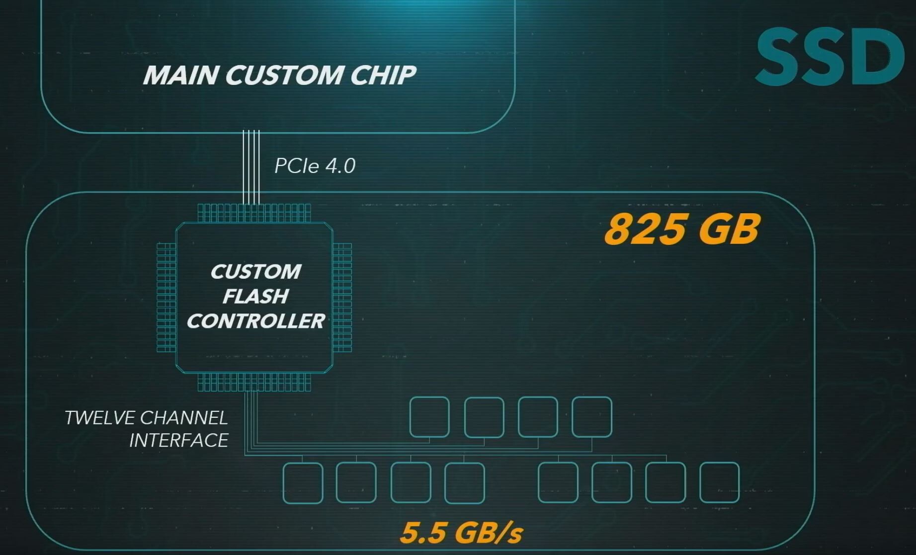
Each PlayStation 5 ships with a PCI-Express 4.0 x4 SSD with a flash controller that has been designed in-house by Sony. The controller features 12 flash channels, and is capable of at least 5.5 GB/s transfer speeds. When you factor in the exponential gains in access time, Sony expects the SSD to provide a 100x boost in effective storage sub-system performance, resulting in practically no load times.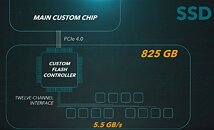
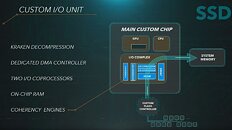
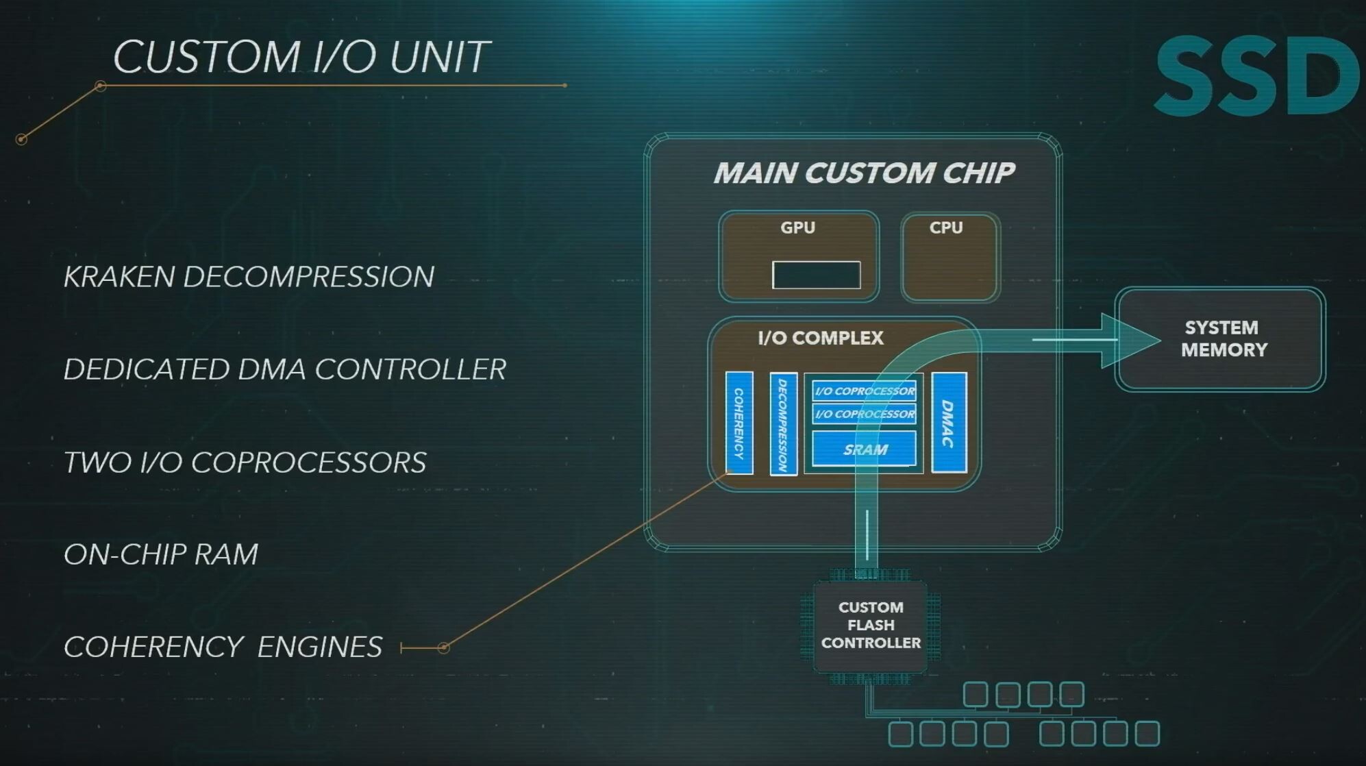
 The secret sauce here is that Sony is using its own protocol instead of NVMe, in supporting 6 data priority tiers versus 2 on NVMe. Each PlayStation 5 ships with an 825 GB SSD, which is expandable using external HDDs over USB, or a selection of third-party M.2 NVMe SSDs certified by Sony. PlayStation 4 games can run directly off your external HDD, but PlayStation 5 games have to be transferred from your HDD to the console's main SSD. Past generations of PlayStation implemented ZLib data compression on Blu-ray and HDD media. PlayStation 5 is implementing Kraken, with hardware-accelerated de-compression via fixed-function hardware built directly into the main SoC.
SoC is where Cerny sounded restrained in what he wanted to disclose. The SoC is a semi-custom chip designed by Sony and AMD, possibly on a 7 nm-class silicon fabrication process. Sony won't specify if it is a monolithic silicon or an MCM, but there are three building-blocks to it: CPU, GPU, and I/O complex. The CPU is based on AMD "Zen 2" x86-64 microarchitecture, and the GPU is based on the company's upcoming RDNA2 graphics architecture.
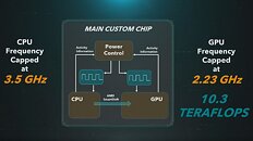
There are eight "Zen 2" CPU cores, although the company didn't mention if SMT is featured. The maximum CPU clock speed is 3.50 GHz. The GPU is a whole different story from the one on the Xbox Series X Velocity Engine semi-custom chip. Sony decided to go with 36 RDNA2 compute units ticking at up to 2.23 GHz engine clock, compared to 52 compute units running at up to 1.825 GHz on the upcoming Xbox. Sony's GPU ends up with up to 10.3 TFLOPs max compute throughput, compared to Microsoft's 12 TFLOPs.
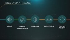
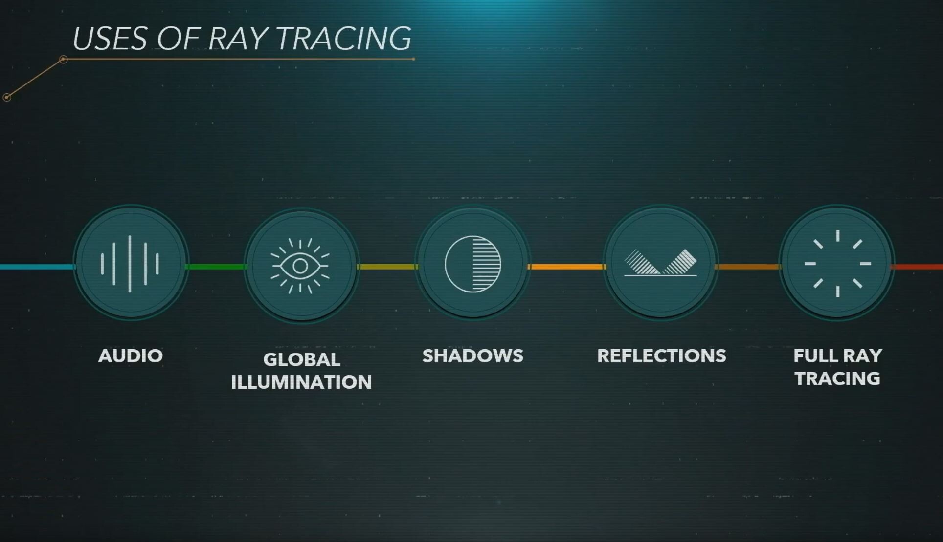
Sony also shed some "light" on the hardware-accelerated real-time ray-tracing approach AMD is taking with RDNA2. Apparently, each compute unit features a hardware component called "Intersection Engine," with roughly the same function as an RT core on NVIDIA "Turing," which is to calculate the intersection of rays with geometry (such as triangles or polygons) in a scene. This combines with a fairly standardized bounding volume hierarchy (BVH) model to achieve a hybrid of ray-traced elements in an otherwise conventional rasterized 3D scene (pretty much where NVIDIA is right now with RTX). On PlayStation 5, RDNA2's ray-tracing hardware is leveraged for positional audio, global illumination, shadows, reflections, and full ray-tracing.
The third key component of the SoC is the I/O complex. This handles all of the chip's I/O, not just with peripherals and video output, but also storage and memory. There are dedicated I/O co-processors on-silicon designed to reduce the various I/O's processing stack on the CPU cores, and reduce latencies at various stages. There's also a certain amount of SRAM that caches transfers between the various components on the I/O complex. The custom chip leverages AMD SmartShift in power-management.
PlayStation 5 uses 16 GB of GDDR6 memory. Sony did not mention the memory clock, bandwidth, or even the memory bus width. It did drop some hints about memory management. It appears like PlayStation 5 does not partition memory the way Xbox Series X does, and possibly sticks to the hUMA model of the PlayStation 4 (using a common pool of physical memory for system- and video memory).
Lastly, a large chunk of Sony's presentation focused on the next frontier for hardware innovation: positional audio. Sony is investing heavily on positional audio that takes into account the gamer's physical HRTF (head-related transfer function). The company is leveraging the vast amounts of CPU power gained from the upgrade to "Zen 2," to achieve this.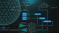 We still don't know what a PlayStation 5 console will look like.
Source:
Sony Computer Entertainment (YouTube)
Each PlayStation 5 ships with a PCI-Express 4.0 x4 SSD with a flash controller that has been designed in-house by Sony. The controller features 12 flash channels, and is capable of at least 5.5 GB/s transfer speeds. When you factor in the exponential gains in access time, Sony expects the SSD to provide a 100x boost in effective storage sub-system performance, resulting in practically no load times.
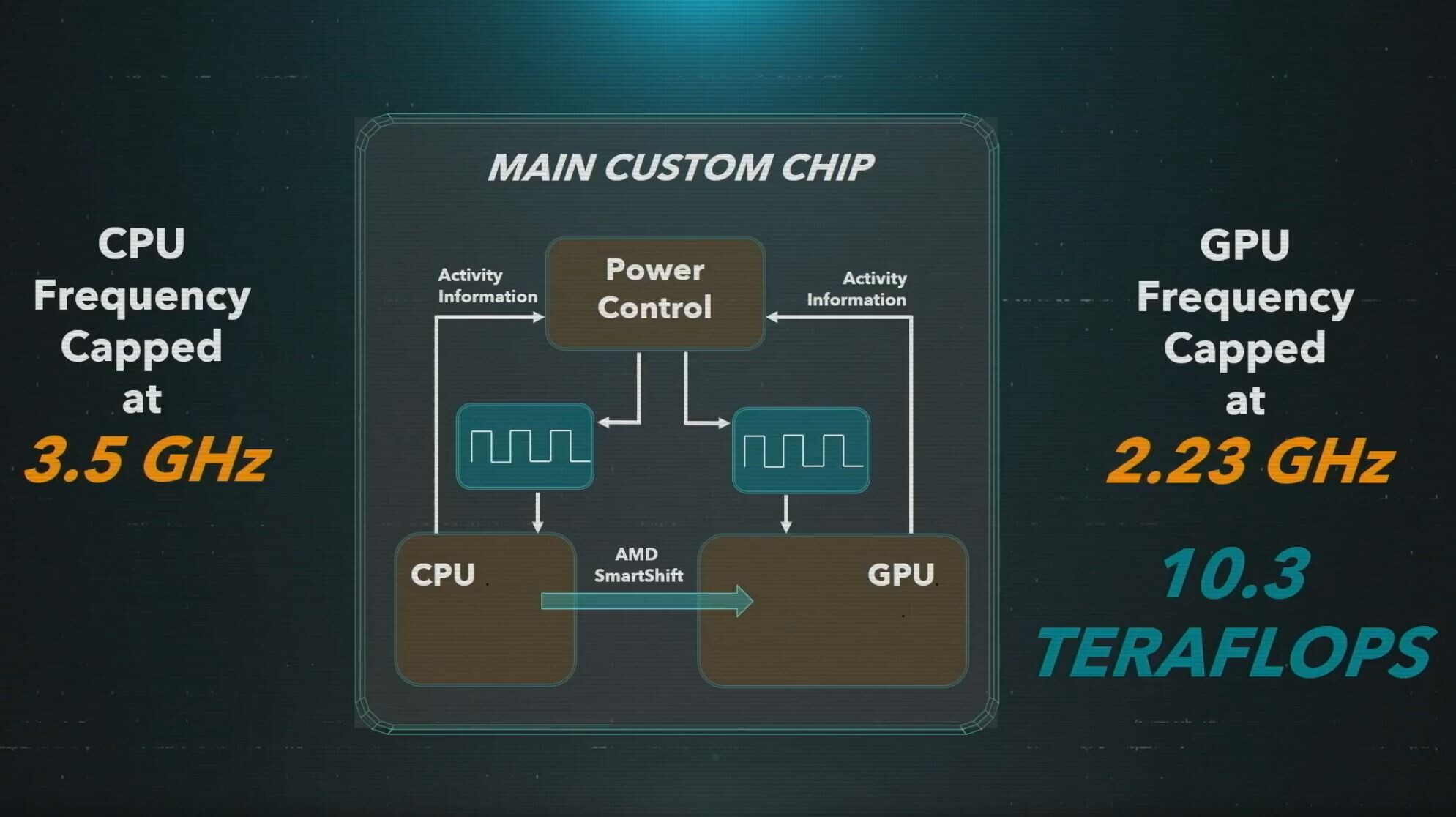
SoC is where Cerny sounded restrained in what he wanted to disclose. The SoC is a semi-custom chip designed by Sony and AMD, possibly on a 7 nm-class silicon fabrication process. Sony won't specify if it is a monolithic silicon or an MCM, but there are three building-blocks to it: CPU, GPU, and I/O complex. The CPU is based on AMD "Zen 2" x86-64 microarchitecture, and the GPU is based on the company's upcoming RDNA2 graphics architecture.
There are eight "Zen 2" CPU cores, although the company didn't mention if SMT is featured. The maximum CPU clock speed is 3.50 GHz. The GPU is a whole different story from the one on the Xbox Series X Velocity Engine semi-custom chip. Sony decided to go with 36 RDNA2 compute units ticking at up to 2.23 GHz engine clock, compared to 52 compute units running at up to 1.825 GHz on the upcoming Xbox. Sony's GPU ends up with up to 10.3 TFLOPs max compute throughput, compared to Microsoft's 12 TFLOPs.
Sony also shed some "light" on the hardware-accelerated real-time ray-tracing approach AMD is taking with RDNA2. Apparently, each compute unit features a hardware component called "Intersection Engine," with roughly the same function as an RT core on NVIDIA "Turing," which is to calculate the intersection of rays with geometry (such as triangles or polygons) in a scene. This combines with a fairly standardized bounding volume hierarchy (BVH) model to achieve a hybrid of ray-traced elements in an otherwise conventional rasterized 3D scene (pretty much where NVIDIA is right now with RTX). On PlayStation 5, RDNA2's ray-tracing hardware is leveraged for positional audio, global illumination, shadows, reflections, and full ray-tracing.
The third key component of the SoC is the I/O complex. This handles all of the chip's I/O, not just with peripherals and video output, but also storage and memory. There are dedicated I/O co-processors on-silicon designed to reduce the various I/O's processing stack on the CPU cores, and reduce latencies at various stages. There's also a certain amount of SRAM that caches transfers between the various components on the I/O complex. The custom chip leverages AMD SmartShift in power-management.
PlayStation 5 uses 16 GB of GDDR6 memory. Sony did not mention the memory clock, bandwidth, or even the memory bus width. It did drop some hints about memory management. It appears like PlayStation 5 does not partition memory the way Xbox Series X does, and possibly sticks to the hUMA model of the PlayStation 4 (using a common pool of physical memory for system- and video memory).
Lastly, a large chunk of Sony's presentation focused on the next frontier for hardware innovation: positional audio. Sony is investing heavily on positional audio that takes into account the gamer's physical HRTF (head-related transfer function). The company is leveraging the vast amounts of CPU power gained from the upgrade to "Zen 2," to achieve this.

178 Comments on Sony Reveals PS5 Hardware: RDNA2 Raytracing, 16 GB GDDR6, 6 GB/s SSD, 2304 GPU Cores
Sony Patent.
esportscontinental.com/playstation-5s-new-dualshock-design-leaked/
Nobody knows how it differs from just buying an equivalent ZEN2 & RDNA2 discrete GPU. They won't be the same in other words.