Monday, September 28th 2026

Panther Lake Teardown Shows Intel 18A Near TSMC N3E, Newer TSMC Nodes Still Ahead
SemiAnalysis has published a teardown of Intel's Panther Lake (Core Ultra 7 365), offering a rare look at 18A inside a shipping chip. Intel's 18A node brings advanced manufacturing technologies such as rear-side power delivery and a new transistor design, so its success is vital for the Foundry. The firm found the 18A compute logic to be similar in density to the TSMC N3E logic used in the 12-core Xe3 GPU tile. It also puts 18A about 18.6% denser than the Intel 3 GPU logic, using a representative-cell model. However, SemiAnalysis says 18A does not lead TSMC N3P, N2, or Samsung SF2 in peak density. It further cautions that whole-die density depends on cell mix and placement.
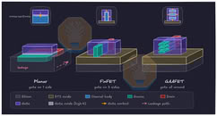
Panther Lake is Intel's first chip with RibbonFET gate-all-around transistors, and the first commercial implementation of PowerVia backside power delivery. SemiAnalysis counted four stacked ribbons per transistor, compared to three sheets on Samsung's SF2. Moreover, the Cougar Cove P-core takes roughly the same area as Lunar Lake's Lion Cove, even though L2 grew from 2.5 MiB to 3 MiB. Panther Lake's NPU 5 reportedly requires 36.9% less chip area than Lunar Lake's NPU 4, though the number of INT8 MAC units remains the same. SemiAnalysis describes the CPU cores as incremental updates.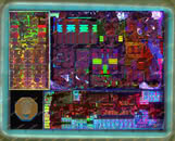
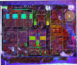
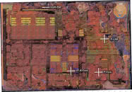 Intel launched Panther Lake at CES 2026, after entering volume production at Fab 52. The 18A compute die has also reached around 80% yield, and Intel is reportedly moving most Nova Lake compute tile production in-house. Per the detailed analysis, Intel looks to be near TSMC N3E territory, while TSMC's newer nodes still hold the density edge. More SemiAnalysis teardowns of Samsung SF2 and TSMC N2 are apparently coming, which should show how 18A stacks up against the newer nodes.

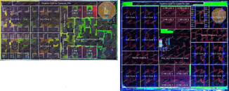
Source:
SemiAnalysis
Panther Lake is Intel's first chip with RibbonFET gate-all-around transistors, and the first commercial implementation of PowerVia backside power delivery. SemiAnalysis counted four stacked ribbons per transistor, compared to three sheets on Samsung's SF2. Moreover, the Cougar Cove P-core takes roughly the same area as Lunar Lake's Lion Cove, even though L2 grew from 2.5 MiB to 3 MiB. Panther Lake's NPU 5 reportedly requires 36.9% less chip area than Lunar Lake's NPU 4, though the number of INT8 MAC units remains the same. SemiAnalysis describes the CPU cores as incremental updates.


26 Comments on Panther Lake Teardown Shows Intel 18A Near TSMC N3E, Newer TSMC Nodes Still Ahead
low power cores, cores with no instruction etc. work very well on a smartphone. I expect something else and much more durable on desktops.
Having read it yesterday I'm quite impressed at how Intel managed to correct their 14/10nm-era fumbles. Them not depending that much on TSMC in the future is good news for all consumers.
@Geddagod this article doesn't mention anything about the library type. Do you think Panther Lake's compute tile is using 18A HP or a mix of 18A HP and 18A HD?
Btw it should be 18AP used not base 18A used in NVL, according to Intel at VLSI.Where?They have had dense and classic cores for a while. Effectively big and small cores. Zen 6 is rumored to bring even smaller core variants for the LPE cores but I forget what the rumors say about them exactly. Totally new arch, cut down Zen 6 arch, same Zen 6 arch with a cut down FPU and even smaller core area?Bringing a Royal Core concept would be them sacrificing a bunch of area for peak 1T perf. We should see what royal core might have looked like at Intel when Ahead Computing releases info about their upcoming core, since that was allegedly the same team developing royal core that left and started their own company when royal core was canned.
Unified Core's goals seem to be fixing the terrible power and poor area problem plaguing Intel's P-cores more than giving a large increase in per-core performance. Hence why it's rumored to be based on scaling up the E-core design, and the team being led by an E-core team architect.Any source for this?
WCL GPU: likely HD
Xe3 IP : 18A, intel 3, N3E
The 5950X with 16 cores came out in 2020 when the 10900K at the time only had 10c/20t. AI was in it's infancy in 2020 and we didn't have ChatGPT yet, it hadn't gone mainstream yet. It was still common to use early AI/ML tools that used both CPU and GPU. Today it's virtually all GPU unless you're into video editing or the like.
Today the 7800X3D system with 8 fewer cores is in no way inferior to the 5950X 16 core one (for me). The 8 extra real cores simply don't help anything for me, not daily driving nor gaming, the 7800X3D is always faster, though not necessarily noticably in all games/apps. Most games I run for instance just run great on both, but newer titles definitely run noticeably better on the 7800X3D and not just loading from the faster NVME. Since 2020 most of the average workload went to the GPU side but Intel is still building CPUs like it's early 2020 chasing higher and higher core counts that almost nobody needs.
It would be one thing if Intel's 24c monsters would be able to boost 8 cores really high when not running highly parallel workloads to beat AMD, but of course that isn't what we see, Intel simply keeps failing in my eyes.
This has nothing to do with other factors, such as the AI workloads you mentioned. I don't know why you're so opposed to more cores. Your computer is constantly performing high-parallelism tasks, and modern game engines also have high parallelism. It can also provide better performance during shader compilation and decompression, all of which benefits you without any harm. You compared zen4x3d with zen3, confusing the comparison targets, which are cpu models from intel and amd of the same generation with similar st performance. While you are opposing core counts, amd increased cpu cores by 50%, aka 1.5x silicon area, does this move you at all.
5950x should not be compared with intel configurations. AMD dual ccd has no game performance improvement compared to single ccd due to dual ccd latency, making it unable to effectively utilize more cores in latency-sensitive applications. Intel provides it within a single compute tile and does not have this problem, so it can bring the performance boost, including in games.
Regarding content humanly perceptible, I believe the gaming advantage of 9800x3d is barely perceptible to humans, for the following reasons.
Its performance advantage applies to high-end gpus, such as 5090, while its advantage under 5070 is close to 1%. Its performance advantage is concentrated in low-resolution high-fps games, and high fps requires a high refresh rate 360hz+ display to be effectively distinguished and utilized by humans, with a difference of less than 1ms. As for display smoothness, nvidia's mfg feature can easily improve aaa game smoothness.
its overclocking potential is lower; in fact, the gaming performance of an unoced 9850x3d is similar to an oced 270k plus, but it is more expensive, and its mt performance is much worse.
To summarize, fully utilizing the gaming performance of 9800x3d requires a gpu above 5080, frequently playing competitive fps games rather than aaa games (the sensitivity to latency for competitive game types other than fps is questionable), being equipped with a very high refresh rate display, and being someone whose competitive level cannot tolerate even 1ms of latency (with mouse and keyboard naturally using the most advanced standards, such as logitech's HITS mouse).
They are serving us server architecture ported for to desktop platforms.
…do you genuinely just not understand how lithography improvements work or are you trolling? Like… what you wrote is nonsense. Yes, individual cores are getting (generally) physically smaller with each iteration. That’s kind of the point.
Not to mention arguing that Intel didn’t have “big cores” since Sandy when Ivy was literally just a die shrink and everything until Skylake and friends was a refinement of that architectural paradigm is kind of wild.