
News Posts matching #2027

Return to Keyword Browsing

ASML Targets 60+ EUV Shipments in 2026 as Memory Demand Surges

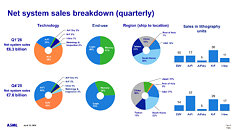
In the latest Q1 2026 quarterly figures, ASML announced plans to ship over 60 EUV units this year, including both High-NA and Low-NA EUV lithography scanners. This is a significant increase from the 48 units shipped in 2025, but it doesn't break any records compared to the company's expectations for 2027. ASML predicts shipping about 80 EUV systems in 2027, driven by massive demand from memory makers. As memory has become the most sought-after commodity in AI data centers, there is simply not enough supply to meet demand. In Q1 2026, ASML reported that nearly half—45% to be precise—of its revenue came from South Korea.

While ASML hasn't provided specific data per manufacturer, we know that South Korean semiconductor makers primarily focus on memory, storage, and to a lesser extent, logic production. More than half of the quarterly shipments, at 51%, are dedicated to memory production. Companies like SK hynix and Samsung are purchasing many EUV systems to support their growing memory and storage businesses, which include the latest technologies like GDDR6, HBM3, HBM4, and DDR4/DDR5, all consumed by AI data centers worldwide. SK hynix plans to install 20 Low-NA EUV units in the next two years, all designed for HBM memory and advanced storage solutions, making SK hynix one of ASML's largest customers.

Apple Ramps Up MacBook Neo Production to 10 Million Units Amid Strong Demand

Apple has informed its supply chain that the company now aims to produce a total of 10 million first-generation MacBook Neo laptops, as consumer demand has been phenomenal. Initially, with the MacBook Neo launch, Apple expected consumers to purchase between 5 and 8 million units throughout the lifecycle of the first generation. However, since demand has exceeded initial expectations, Apple is significantly increasing production to meet this demand. As the Cupertino-based company has access to a wide network of manufacturing partners, ramping up production is straightforward, provided the main component—the A18 Pro SoC—is consistently supplied by TSMC.

Additionally, Apple is already planning a second-generation MacBook Neo with major upgrades to the overall system, primarily due to the new A19 Pro SoC, which will come with 12 GB of RAM. The current MacBook Neo features the mobile A18 Pro chip and is limited to 8 GB of RAM. According to recent rumors, Apple may upgrade the MacBook Neo's internals in 2027, equipping it with an A19 Pro, the same SoC found in the latest iPhone 17 Pro smartphones. Inside the MacBook Neo, Apple has opted to reuse the iPhone 16 Pro's chip, which is produced by TSMC and includes 8 GB of LPDDR5X memory. This memory is directly attached above the A18 Pro SoC using Integrated Fan-Out Package on Package (InFO-PoP) technology, creating a 3D wafer-level fan-out package.

Rumor Tips A19 Pro SoC and 12 GB RAM for Apple MacBook Neo

The Apple MacBook Neo has been a bit of a shock to system in the laptop world, thanks to its low barrier to entry and surprisingly solid performance for everyday tasks. However, one of the biggest criticisms levelled against the MacBook Neo is its mobile A18 Pro chip and limited 8 GB of RAM. According to recent rumors, though, Apple may upgrade the internals in the MacBook Neo in 2027, bumping it up to an A19 Pro, which is the SoC featured in the latest iPhone 17 Pro smartphones.

The A19 Pro is still a mobile SoC, and it is slated to use the same 5-core GPU configuration as the A18 Pro in the current MacBook Neo, but that SoC upgrade also means that the MacBook Neo would no longer be limited to just 8 GB of LPDDR5X. Instead, as the rumors suggest, the MacBook Neo 2027 will see a 50% memory increase to 12 GB total memory. So far, the MacBook Neo seems to have been such a hit in sales that the Cupertino giant has already started increasing production of the laptop.

SEMI Projects Double-Digit Growth in Global 300 mm Fab Equipment Spending for 2026 and 2027

Worldwide 300 mm fab equipment spending is expected to increase 18% to $133 billion in 2026 and 14% to $151 billion in 2027, SEMI reported today in its latest 300 mm Fab Outlook. This strong growth reflects surging AI chip demand for data centers and edge devices, as well as the growing commitment to semiconductor self-sufficiency across key regions through localized industrial ecosystems and supply chain restructuring. Looking further out, the report projects investment will continue to increase 3% to $155 billion in 2028 and another 11% to $172 billion in 2029, respectively.

"AI is resetting the scale of semiconductor manufacturing investment," said Ajit Manocha, President and CEO of SEMI. "With global 300 mm fab equipment spending projected to exceed $150 billion in 2027 for the first time, the industry is making historic, sustained commitments to the advanced capacity and resilient supply chains needed to power the AI era."

NVIDIA's "Rubin Ultra" Reportedly Faces Issues With CoWoS-L Packaging

NVIDIA is reportedly experiencing manufacturing issues with its next-generation "Rubin Ultra" GPU design, one of the company's most ambitious chip development projects, due to the limitations of modern packaging technology. The world's largest company is already shipping customer samples of the standard "Rubin" GPUs, with mass shipments set to begin this summer. However, the current roadmap for the upgraded "Rubin Ultra" design may be encountering technological limitations, as NVIDIA's design goals are too ambitious for TSMC's packaging capabilities. Reportedly, NVIDIA plans to double the regular "Rubin" two-die package with 8 HBM4 modules into a new "Rubin Ultra" package that will include four silicon dies and 16 HBM4E modules in a single package. This configuration is scheduled for 2027, but the sheer volume of silicon may be too much for TSMC's packaging, according to Global Semi Research.

In a typical CoWoS package, TSMC usually combines multiple smaller dies and multiple HBM memory modules into a unified package that supports the entire AI build-out. However, with the ambitious "Rubin Ultra" design, NVIDIA planned to use CoWoS-L, which was expected to handle the design and concept that "Rubin Ultra" was based on. It is rumored, however, that in a 2+2 die package—meaning four dies as in this architecture—TSMC is encountering warping issues. The package—which includes a substrate—is bending in multiple directions, causing the compute dies of "Rubin Ultra" to not make complete contact with the underlying substrate. This instability means that TSMC has to explore alternatives within its packaging portfolio. One of these alternatives is a panelized approach called CoPoS, which stands for Chip-on-Panel-on-Substrate.

Samsung Readies PCIe 5.0 QLC SSD with a Custom RISC-V Controller

Samsung has developed a new SSD controller based on the open-source RISC-V instruction set, moving away from the Arm ISA in some of its SSD controllers. With the introduction of the BM9K1 PCIe 5.0 QLC NAND SSD, Samsung has officially created a proprietary RISC-V IP that will serve as a foundation for many SSDs the company plans to release. Announced at the China Flash Market Summit 2026, the BM9K1 SSD has been showcased with just one metric: sequential read speed. Achieving a maximum sequential read speed of 11.4 GB/s, Samsung has reached impressive speeds for QLC NAND Flash. While the sequential write speed is unknown, it is expected to be around 10 GB/s, varying slightly depending on Samsung's design. Typically, high-performance SSDs use TLC NAND, as seen in Samsung's own 9100 Pro SSD, which we reviewed. It features 3D TLC V-NAND V8 with 236 layers. While this SSD uses TLC NAND and has a proprietary Samsung Presto 5 nm controller running on Arm-based cores, Samsung might transition a significant portion of its SSD lineup to a RISC-V based design with the BM9K1, offering satisfactory performance with QLC NAND.

Interestingly, Samsung has designed this SSD with considerations for size, power, and AI. For instance, the BM9K1 PCIe 5.0 SSD replaces the previous BM9C1 PCIe 4.0 SSD controller. Although both use QLC NAND, the newer BM9K1 features a new RISC-V controller and a fresh PCIe 5.0 interface, doubling the performance in sequential reads on average. The power efficiency of the new RISC-V design is also improved. Samsung claims a 23% increase in power efficiency, thanks to the flexibility of RISC-V, which allows for greater customization and optimization of the controller firmware to match I/O patterns with the QLC NAND, resulting in nearly a quarter less power consumption. This improvement is expected to have a significant impact on small form factor PCs and client laptops. The main drawback of the design is the use of QLC NAND, but Samsung may introduce TLC NAND SSDs with RISC-V controllers in the future. For now, these remain on the 5 nm Presto Arm-powered controllers.

Nintendo Plans Switch 2 With User-Replaceable Batteries for EU

Recent right to repair laws passed in the EU demand that, starting in February 2027, electronic devices have batteries that are user-replaceable with commonly available tools and without risk to the end user—that is to say, they shouldn't require proprietary tools or tools that aren't available to consumers. Nintendo, for its part, already preparing an update to the Nintendo Switch 2 to comply with this law, according to a report by Nikkei (via Covergeek), although the exact details of the more repairable battery model is unknown at the time of writing. According to the report, the more repairable Switch 2 will only launch in Europe, but Nintendo would expand the hardware to different regions as required by law.

In iFixit's teardown of the Nintendo Switch 2 and its battery replacement guide for the Switch 2 Joy Cons, the organization noted that the battery for both the Switch 2 and its Joy Cons were adhered in place, and a spudger was required to remove the batteries from the devices. While this isn't necessarily a specialized tool, it could be argued that needing to either dissolve an adhesive or pry a battery loose could add additional risk to the end user. To this end, it seems likely that both the Switch 2 and its Joy Cons could see a revision with weaker adhesive or no adhesive at all, which would make battery replacements easier and safer. It could also mean that Nintendo will need to replace the tri-point screws that hold the Switch 2 together.

Strong AI Momentum to Drive 24.8% Growth in Foundry Revenue in 2026

TrendForce's latest research on the foundry industry reveals that continued investment in the AI arms race by North American CSPs and AI startups will keep demand for AI processors and supporting ICs strong in 2026. Global foundry revenue is projected to grow 24.8% YoY to approximately US$218.8 billion, with TSMC expected to post the largest increase of around 32% YoY.

Demand for advanced nodes will continue to be driven by AI GPUs from companies such as NVIDIA and AMD. Meanwhile, North American CSPs, including Google, AWS, and Meta, and AI startups such as OpenAI and Groq, are accelerating the development of their own AI chips. Many of these designs are expected to enter volume production and begin shipping in 2026, becoming key drivers for 5/4 nm and more advanced process technologies.

AMD "Medusa Point" APU Early Benchmarks Match "Strix Point" at Half the Clock Speed

AMD is preparing to launch its "Medusa Point" APU in early 2027. However, more benchmarks are emerging to showcase what the actual SoC can do as AMD and its OEM partners test the chip. In the latest Geekbench v6 run, AMD's 10-core, 20-thread "Zen 6" chip appeared with the AMD Engineering Sample number 100-000001713-21_N, achieving a 2,300 single-core and 13,002 multicore score while officially running at only a 2.4 GHz base frequency. In real-world operation, it ran within the range of 2.0-2.1 GHz during the benchmark. The most surprising factor is that this "Medusa Point" test system can match a 10-core, 20-thread AMD Ryzen AI 9 365 "Strix Point" APU that operates at more than double the frequency. When comparing the two, "Medusa Point" scores slightly lower in single-core performance, while the multicore score is surprisingly higher.

This phenomenon could be attributed to the fact that the "Zen 6" cores in the "Medusa Point" APU are much better performing and more optimized for the workloads that Geekbench tests. The IPC improvement target from "Zen 5" in "Strix Point" to the newest "Zen 6" could be a high single-digit to low double-digit gain on average. It is likely that the combination of new instructions and IPC improvements is what is pushing "Medusa Point" so high. Since the new APU also appeared in firmware running AVX-VNNI in FP16 precision, we might be seeing these workloads getting accelerated thanks to the lower precision of the floating-point operations. For now, the situation remains a mystery, at least until more benchmarks are available in the coming months. AMD is expected to launch this new APU around CES 2027, so we still have a lot of time before official and third-party benchmarks are released.

Xbox Confirms Helix Dev Kits To Land End 2027, Xbox Mode Arrives in Windows 11 in April

Asha Sharma, the new CEO of Xbox, recently announced that the next-gen Xbox gaming console is called the Xbox Helix—at least for the time being—and hinted that more information would be revealed about the upcoming Xbox at GDC 2026. Now, GDC is here, and Xbox has delivered on that hint, with Xbox VP of Next Generation, Jason Ronald, divulging more information about Project Helix in a panel. The most notable piece of information that emerged about the console is that alpha versions of Helix dev kits would start shipping to customers as early as the end of 2027. This more or less confirms the recently rumored 2027-2028 launch window of the next-gen Xbox.

Ronald also reiterated that the next-gen Xbox is "designed to play your Xbox console and PC games," although it's still somewhat unclear if Helix will be a full-fledged console-PC hybrid à la Valve's Steam Machine—although rumors suggest that this will be the case. The executive also confirmed that it is working with AMD on a slew of new machine learning-powered tech, including FSR Diamond, which AMD also announced at GDC, and that the new AMD SoC would be designed around upcoming DirectX versions for improved ray tracing, performance, and efficiency. He also confirmed that the Helix will continue the backwards compatibility trend that Xbox has become known for, promising that Xbox will continue to play games made for the last four generations of consoles. Presumably, this means that the Helix will be able to play games from the Xbox Series, Xbox One, and Xbox 360 generations as well as games designed for the Xbox Helix.

AMD Prepares "FSR Diamond" Update for Xbox Project Helix

AMD is reportedly developing a next-generation FSR update, codenamed "FSR Diamond," for the upcoming Xbox project "Helix" gaming console. With the Project Helix console expected to launch in 2027, the details of "FSR Diamond" remain a mystery. It's unclear what AMD aims to achieve with this AI-powered video generation technology, but it likely builds on previous advancements like Radiance Caching and Ray Generation, adding a new dimension to the company's graphics capabilities. We might see an AMD equivalent of the multi-frame generation technology found in NVIDIA's GeForce RTX 50-series GPUs and Intel's XeSS 3.0. Since Project Helix is anticipated to feature RDNA 5 / UDNA graphics IP, this feature could be exclusive to that generation, as AMD tends to tie its latest technologies to the current RDNA IP.

AMD already differentiates its latest FSR "Redstone" suite of technologies, with features like Ray Regeneration and Radiance Caching exclusive to RDNA 4 hardware in the Radeon RX 9000 series of GPUs. Other basic technologies, such as upscaling and frame generation, are supported on older RDNA 3/2/1 generations but use an FSR 3.1 fallback, with no FSR 4 support currently available. However, since INT8-based FSR 4 exists, it may only be a matter of time before the company extends this capability to older GPUs, though the expected performance might not be optimal. For multi-frame generation and potentially dynamic multi-frame generation, "FSR Diamond" would need specialized hardware. Even NVIDIA, with its MFG 6x mode and Dynamic MFG, keeps those features exclusive to the GeForce RTX 50-Series "Blackwell," which uses hardware flip-metering available only on the newest GPU generation. Similarly, RDNA 5 / UDNA could incorporate these hardware components as well.

Intel "Nova Lake-S" Appears with B960 Chipset and Support for DDR5-8000

Intel's upcoming "Nova Lake-S" has been spotted in the wild for the first time. During the Embedded World 2026 event, German media outlet ComputerBase spotted an Intel Core Ultra 400 series "Nova Lake-S" mini-PC, featuring Intel's upcoming B960 chipset and support for DDR5 memory running at 8,000 MT/s. This suggests that Intel is upgrading its integrated memory controller on the "Nova Lake" platform to support these DDR5 speeds before any XMP and factory-overclocked memory are used. The support for higher-speed memory indicates that even Intel's current memory controller, which reportedly achieves DDR5 speeds of 7,200 MT/s in the upcoming "Arrow Lake Refresh," will receive an upgrade alongside the new core IP and configuration.

Speaking of configurations, ComputerBase confirmed that the 52-core top SKU of "Nova Lake" will have a TDP of 175 W, while other configurations with a TDP of 65 W will also be available. This is a significant boost of the base TDP rating that Intel is delivering, as the current flagship "Arrow Lake" Core Ultra 9 285K carries a base TDP of 125 W, a whole 50 W less. As this CPU is a 52-core model in its top-configuration, boost frequencies are going to push the power usage much higher as the processor runs a heavier load. Graphics output is powered by Xe3P GPU IP, as previously rumored, confirming that Intel's next-generation graphics is there. For AI capability, "Nova Lake" will deliver more than 100 TOPS using the 8-bit INT8 data type, thanks to the onboard NPU and the powerful Xe3P GPU IP.

Fujitsu Showcases "MONAKA" CPU Sample with 3.5D XDSiP Packaging

During MWC, Fujitsu partnered with networking equipment maker 1FINITY to unveil the first silicon wafers and an engineering sample of its "MONAKA" CPU. Scheduled for release in 2027, the initial Fujitsu MONAKA CPU utilizes the Armv9-A architecture and a 3D chiplet layout that combines a core die with separate SRAM and I/O dies. A single chip features 144 cores, and two-socket configurations can scale up to 288 cores per node. The platform supports 12-channel DDR5, PCIe 6.0 with CXL 3.0, and Arm SVE2 for AI and HPC workloads. Fujitsu has chosen TSMC to manufacture this chip using the 2 nm node, paired with Broadcom's 3.5D eXtreme Dimension System-in-Package (XDSiP) packaging architecture. This packaging allows MONAKA to become a 144-core design featuring four 36-core chiplets. These chiplets are stacked face-to-face with SRAM tiles through hybrid copper bonding, utilizing TSMC's N5 process for the cache layer.

In the pictures below, we can see the silicon complex in its early sample packaging, which shows a large central I/O die, HBM memory around the CPU, and the new packaging technology. Reportedly, this CPU has already reached a working version, with Broadcom shipping the CPU to Fujitsu in late February this year. After initial testing and early performance validation, Fujitsu plans to ship these processors to customers around summer, with mass shipping to commence in 2027. The company envisions this SoC as a powerhouse for AI inference, simulation, and large-scale data processing. It will sell these systems to external customers, who showed great interest in Fujitsu's A64FX when the Fugaku computer came online. Fugaku was the most powerful supercomputer back in 2020, achieving 415.53 PetaFLOPS of FP64 and an impressive HPL-AI score of 1.421 ExaFLOPS using lower FP16 precision. Hence, we expect the new MONAKA CPU to enable much greater speeds and some efficiency improvements as well.

Resident Evil 1 Remake May Be on the Cards

Resident Evil Requiem recently launched as the newest installment in Capcom's zombie horror franchise, and although it received glowing reviews, even topping the Steam charts and handily beating out every other Resident Evil game on PC, gamers were a little disappointed to find out that the game was originally meant to feature a return to Raccoon City and the Spencer mansion from Resident Evil 1. According to prominent game leaker, Dusk Golem on X, part of the reason for the mansion scene being cut from Requiem was to avoid repetition in both the upcoming Code Veronica remake and a Resident Evil 1 remake.

[Editor's note: Our in-depth review of Resident Evil Requiem is now live]

According to the leaker, Resident Evil 1 is confirmed as being in early development, and a Code Veronica will be the next game in the series, which would mean having gameplay in the same mansion in three successive games, which, in the leaker's own words would "start to feel very samey & not very special at all." Resident Evil Code Veronica Remake is slated to launch in 2027, although the Resident Evil 1 remake is still in the early stages of development, so it seems like a 2029 release date would be the earliest we can expect. Supposedly, the remake will be in the updated RE Engine in which Requiem was also made and demonstrates decent visuals and performance, even with modest hardware requirements.

TSMC Urging Customers to Apply for N2 Node Allocation as it's Almost Full Until 2027

According to Culpium—written by ex Bloomberg tech industry writer Tim Culpan—TSMC is now telling its customers to apply for production allocation for its N2 node, as most of it has already been booked up until the end of 2027. Lead time is said to be six quarters on what production capacity is left, which is causing problems for companies that manufacture with TSMC to live up to their own roadmaps. Even those lucky enough to have been allocated production on the N2 node are said to be looking at as much as a 12 month lead time from start of production until delivery of the finished chips.

Culpium also confirms that NVIDIA now is TSMC's biggest customer, as we reported last week. Even so, NVIDIA is also said to be affected by the N2 node production constraints, even though they might not be as badly affected as small customers of TSMC. The report mentions that there are some exceptions to the lead times, including what is referred to as hot lots or hot runs, but these come in at premium pricing for the customers, as these are last-minute production runs that don't have guaranteed lead times. This is bad news all around, as it means a lot of planned products are unlikely to see the light of day, as they will either be too costly to manufacture or it will simply take too long for it to make sense to invest in.

Nintendo Announces Pokémon Winds and Waves for 2027 Switch 2 Launch

Nintendo has officially announced Pokémon Winds and Pokémon Waves as the latest installment in its never-ending creature-capture series. The two new games will introduce Generation 10 Pokémon and be available exclusively for the Nintendo Switch 2 sometime in 2027. It will be the first Pokémon game exclusive to the Switch 2, and there's no word on whether it will launch for the original Switch or Switch OLED later down the line. An exact launch date was not revealed, although late 2027 seems likely based on previous launches.

The reveal trailer—which is not actual gameplay footage—shows a continuation of the 3D aesthetic, revealing the usual selection of biomes, including oceans, grasslands, rock outcroppings, dungeons, and forests. The trailer also gave us a glimpse at the three new starter Pokémon, Browt, the Grass type, Pombon, the Fire type, and Gecqua, the Water type. The trailer also teased underwater exploration, and what looks like an island resort or town sort of in the style of hut-over-water buildings typically found in calm tropical waters.

Rapidus Secures $1.7 Billion in Funding to Back 2 nm Mass Production Plans by 2027

Rapidus has closed a 267.6 billion yen ($1.7 billion) funding round, pulling in money from both the Japanese government and a broad group of private companies. On the public side, 100 billion yen ($641 million) came from the Information-Technology Promotion Agency (IPA), following a formal selection process run by Japan's Ministry of Economy, Trade and Industry last autumn. Rapidus applied and was picked as the designated operator in November 2025, and the investment followed from there. The remaining 167.6 billion yen ($1 billion) came from 32 private-sector companies, a list that reads like a who's who of Japanese industry: Canon, Fujitsu, Sony, NTT, SoftBank, Honda, Kioxia, Denso, and Toyota are among the names involved, alongside banks, trading companies, and various tech firms (i.e., IBM Japan). Combined with the 7.3 billion yen raised at the company's founding, Rapidus now has a total stated capital of just under 275 billion yen ($1.76 billion).

Rapidus has already taped out a 2 nm GAA test chip using ASML EUV tools in August last year. The company's 2HP process is shaping up to be genuinely competitive, claiming a transistor density of 237 MTr/mm². The goal hasn't changed: get from R&D to full mass production of 2 nm chips by 2027 at the IIM-1 fab in Chitose, Hokkaido, located in northern Japan with around 25,000 wafers per month. Rapidus says it will keep raising money through a mix of public and private sources as it works toward that target.

Running With Scissors Reveals Flesh & Wire, New IP Coming in 2027

Running With Scissors, the (in)famous creator of the POSTAL series, which has amassed millions of fans over nearly three decades, announces its first-ever spinoff title. Flesh & Wire, a dark and violent return to POSTAL's original theme and setting, will arrive on PlayStation 5 and PC via Steam and GOG in 2027, as revealed in the IGN Fan Fest showcase.

Join forces with Angel, a seemingly normal college student suddenly swept up in a fever dream of conspiracy, blood, and vengeance. Along with her loyal sphinx cat Solomon, Angel runs afoul of the law, military, and an ominous cult. Discover the truth about her connection to the events of the first POSTAL game - and seek revenge on the series' protagonist, a man dubbed the Postal Dude.

Intel "Nova Lake-S" Coming in 2027, CES Launch Alongside AMD "Olympic Ridge" Likely

It was revealed in a recent leak that the next-gen AMD Zen 6 Ryzen CPUs would be delayed until 2027, and it has now emerged, that the upcoming Intel "Nova Lake-S" Core Ultra Series 4 CPUs may be joining AMD for an early 2027 launch, when previous reports placed the launch in late 2026. The news comes by way of ubiquitous leakers, HXL on X and Golden Pig Upgrade on Weibo, who say that a CES 2027 launch seems likely for both new CPU generations.

Previously, we got a taste of what to expect from Nova Lake-S in a series of leaks and rumors, which pointed to increased NPU performance as well as core counts that range from 12 on the low-end (4 P-cores, 4 E-cores, 4 LP-cores) to 52 on the high-end (16 P-cores, 32 E-cores, 4 LP-cores). Obviously, these are early leaks, and the official launch is still a way out, so dates may still change, but it seems as though the current silicon and DRAM shortages may result in the lengthening of product launch cycles across the PC industry in general—an outcome that was previously predicted.

AMD Instinct MI455X Reportedly Facing Delays, Only Low-Volume Production This Year

According to SemiAnalysis, which recently released its InferenceX benchmark comparing the inference performance of the latest AI accelerators, AMD's next-generation Instinct MI455X accelerators, designed to compete with NVIDIA's "Vera Rubin," are facing serious manufacturing difficulties, causing delays in AMD's roadmap execution. Only low-volume production will occur this year, while customers will be generating AI tokens in Q2 2027. This means that NVIDIA's "Vera Rubin" VR200 rack-scale system will be the most powerful system shipping this summer, without competition. As AMD's first rack-scale system, the "Helios" AI rack with the MI455X UALoE72 configuration packs 72 GPUs and 6th Gen AMD EPYC "Venice" CPUs in a heterogeneous system designed to run as a single homogeneous GPU, delivering massive AI performance with multi-ExaFLOP compute output.
SemiAnalysisEngineering samples and low volume production of AMD's first rack scale MI455X UALoE72 system will be in H2 2026 while due to manufacturing delays, the mass production ramp and first production tokens will only be generated on an MI455X UALoE72 by Q2 2027.

Sony Could Push PlayStation 6 to 2028/2029 Due to Rising Memory Costs

Sony is reportedly postponing the launch of its next-generation PlayStation 6 console to 2028 or 2029 due to the massive rise in memory costs. This is reportedly impacting decision-making at the top of the company unit responsible for PlayStation strategic planning. Rising memory costs and a tight semiconductor supply chain are the core reasons behind any changes. Initially, we expected to see the wave of next-generation consoles in 2027, as AMD recently confirmed Microsoft's next-generation Xbox arriving in 2027. However, Sony could be abandoning the 2027 release window and pushing its PlayStation 6 console to a late 2028 or even 2029 launch, indicating that the company is not capable of securing sufficient DRAM allocation from its partners. This could leave Microsoft's new Xbox console as superior for an entire year or even two before Sony could join the next-generation console wars.
BloombergSony Group Corp. is now considering pushing back the debut of its next PlayStation console to 2028 or even 2029, according to people familiar with the company's thinking. That would be a major upset to a carefully orchestrated strategy to sustain user engagement between hardware generations.

Intel Confirms Data Center GPU IP After Xe3P with "Xe Next"

Intel has once again confirmed its product roadmap for the next generation of graphics IP, despite rumors that there might not be anything new after the launch of the Xe3P. According to a new presentation from Intel's Anil Nanduri, Vice President of GTM & Product Management AI Accelerators, responsible for data center AI accelerators, Intel will have a dedicated graphics portfolio after the recently introduced "Crescent Island." Labeled as "Xe Next," the next generation of GPU IP is still under development and currently without an official name. It is expected to follow the rollout of the Xe3P-based "Crescent Island" inference-focused GPUs. With "Xe Next," the data center lineup is seemingly expanding into two production lines: inference-focused "Crescent Island" GPUs and the long-awaited "Jaguar Shores" GPU for AI training and HPC workloads.

For AI training and HPC workloads, Intel's "Jaguar Shores" design is reportedly being finalized and will be completed by the middle of this year, with production starting shortly after. Assuming a perfect design, we could see Intel's "Jaguar Shores" GPU late this year or early 2027. It will likely involve a mix of Intel's internal production in collaboration with TSMC or Intel's pure 18A design, assuming yields are manageable. We have already seen that Intel confirmed HBM4 memory will be used in these accelerators, and SK hynix appears to be the main partner supplying Intel with this memory. As a rack-scale design, Intel will compete with NVIDIA and AMD in the highest-margin business.

Wistron Chairman Says AI is Not a Bubble

Simon Lin, the chairman of Wistron, has gone on record to say that AI is not a bubble and that the growth of AI-related orders for the company will be higher in 2026 than those it had in 2025. Reuters is quoting him saying "We believe AI really does help all industries, so I don't think it's a bubble; I think it will mark a new era. A new AI era is arriving." Wistron is expecting AI-related orders to see them through all the way into 2027 and this year's growth is expected to be "significant."

Wistron is expecting to open its new US manufacturing facility this half of 2026, where the company will be producing AI servers on behalf of NVIDIA. Wistron is said to have a four-year contract with NVIDIA that is valued at as much as US$500 billion. The question here is if the industry is trying its best to make as much profit out of the current market trend, or if this really is a long-term business for companies such as Wistron. We've seen past bubbles where company leadership has denied it being a bubble, until it was, but maybe it's different this time around.

AMD Confirms Steam Machine in Early 2026, Xbox SoC Powered by RDNA 5 in 2027

AMD posted its record fourth quarter revenue of $10.3 billion in 2025, and during the earnings call, the company issued some guidance on the upcoming product portfolio. During the call, AMD confirmed that Valve's Steam Machine is on track and shipping early this year, while its custom SoC division that designs processors for PlayStation and Xbox consoles will deliver an RDNA 5-based SoC for the next-generation Xbox console. While the Steam Machine specifications are confirmed, Xbox "Magnus" SoC is still largely a collection of rumored specifications. The "Magnus" SoC is rumored to feature the largest APU ever designed for a consumer console, with a 408 mm² chiplet design. Of this, 144 mm² is dedicated to the SoC built on TSMC's N3P node, while the GPU occupies 264 mm². The AMD chip is expected to include up to 11 CPU cores—three Zen 6 and eight Zen 6c—alongside a substantial GPU setup with 68 RDNA 5 compute units, four shader engines, and at least 24 MB of L2 cache. Memory might expand to 48 GB of GDDR7 on a 192-bit bus. A dedicated NPU is rumored to offer significant on-device AI performance, with reports suggesting up to 110 TOPS.
Dr. Lisa Su, AMDFor 2026, we expect semi-custom SoC annual revenue to decline by a significant double-digit percentage as we enter the seventh year of what has been a very strong console cycle. From a product standpoint, Valve is on track to begin shipping its AMD-powered Steam Machine early this year, and development of Microsoft's next-gen Xbox featuring an AMD semi-custom SoC is progressing well to support a launch in 2027.

Western Digital Unveils New Hard Drive Solutions on its Innovation Day

At its Innovation Day 2026, Western Digital today unveiled a new customer-centric storage roadmap that reinvents the hard drive for AI needs, reinforcing its position as a strategic storage infrastructure partner for the AI-driven data economy. The announcements reflect how WD's fundamental business transformation has enabled a new generation of storage technologies spanning scalable capacity, breakthrough performance optimizations, power efficiency innovations and an intelligent platform API with cost-effective economics.

As AI generates massive amounts of data, it has spurred intense demand for data storage. To meet the moment, WD has focused deeply on customer needs, particularly capacity with proven reliability and economics, performance, power efficiency, and faster qualifications without customer business disruptions. During its Innovation Day, WD showcased technologies that address these essential customer requirements and will deliver them at scale.
Return to Keyword Browsing
Nov 11th, 2026 06:15 CST change timezone

New Forum Posts

Popular Reviews

TPU on YouTube

Controversial News Posts